DP84902 1 7 Encoder Decoder Circuit
June 1994
DP84902
1 7 Encoder Decoder Circuit
General Description
The DP84902 is designed to perform the encoding and de-
coding for disk memory systems It is designed to interface
directly with Integrated Read Channel Products (such as
National Semiconductor鈥檚 DP84910) and with Disk Data
Controller Products with a 2-bit NRZ interface (such as Na-
tional Semiconductor鈥檚 Advanced Disk Controllers) This
Encoder Decoder (ENDEC) circuit employs a 2 3 (1 7) Run
Length Limited (RLL) code type and supports the hard sec-
tored format
The DP84902 has the option of selecting either TTL or ECL
compatible code output to interface with preamplifiers com-
monly used in high data rate applications This is accomm-
plished by the setting of a bit in the control register
The ENDEC also includes write data precompensation con-
trol circuitry which detects the need for write precompensa-
tion This circuitry issues early and late output signals nec-
essary for precompensation The precompensation informa-
tion is generated against a 2T pattern The precompensa-
tion circuitry can be bypassed by the setting of a bit in the
control register
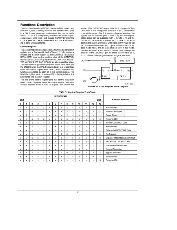
A control reigster is included to configure the ENDEC and to
select device operation options such as output code inver-
sion differential code output bypassing of the encoder and
the use of an internal write clock
The DP84902 is available in 20-pin SO and 20-pin SSO
packages
Features
Y
Y
Y
Y
Y
Y
Y
Y
Y
Y
Y
Operates at 2-bit Non-Return to Zero (NRZ) Data Rates
up to 50 Mbits second
Single
a
5V Power Supply Operation
Low Power Dissipation when TTL compatible code out-
put is selected 150 mW at 50 Mbits second NRZ Rate
TTL Compatible Inputs and Outputs
ECL Compatible Code Outputs (patented) are control
register selectable
Two-bit NRZ Interface
Supports Write Data Precompensation with Early and
Late output signals
Selectable use of either an Internal or External Write
Clock
Power Down Mode Included
DC-Erasure is available to support Analog Flaw Map-
ping Testing
Bypass Mode available which permits Un-Encoded Test
Patterns to be issued at the CODEOUT Pin
Block Diagram
TL F 11963 鈥?1
FIGURE 1 DP84902 ENDEC Block Diagram
TRI-STATE is a registered trademark of National Semiconductor Corporation
IBM is a registered trademark of International Business Machines Corporation
C
1995 National Semiconductor Corporation
TL F 11963
RRD-B30M105 Printed in U S A


 1
1
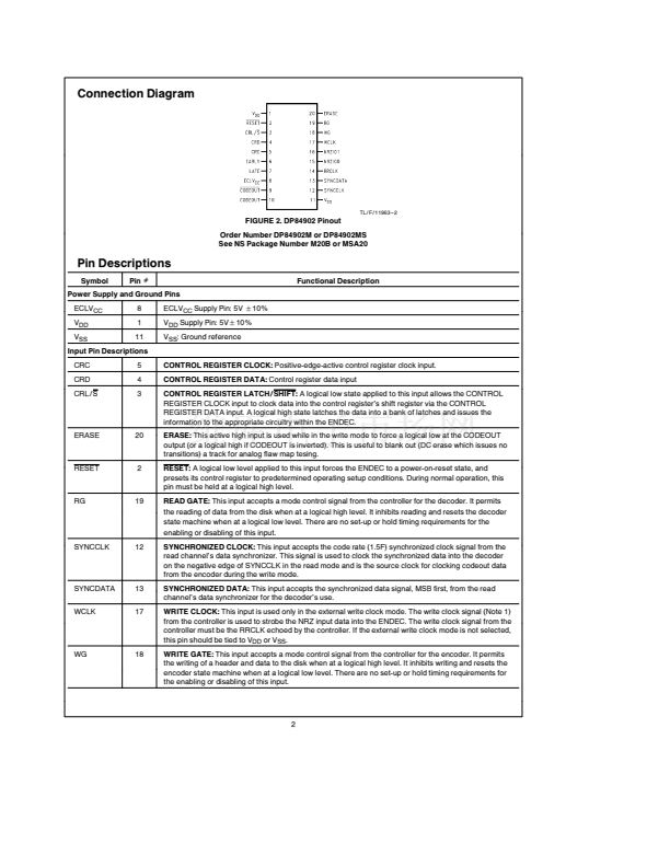 2
2
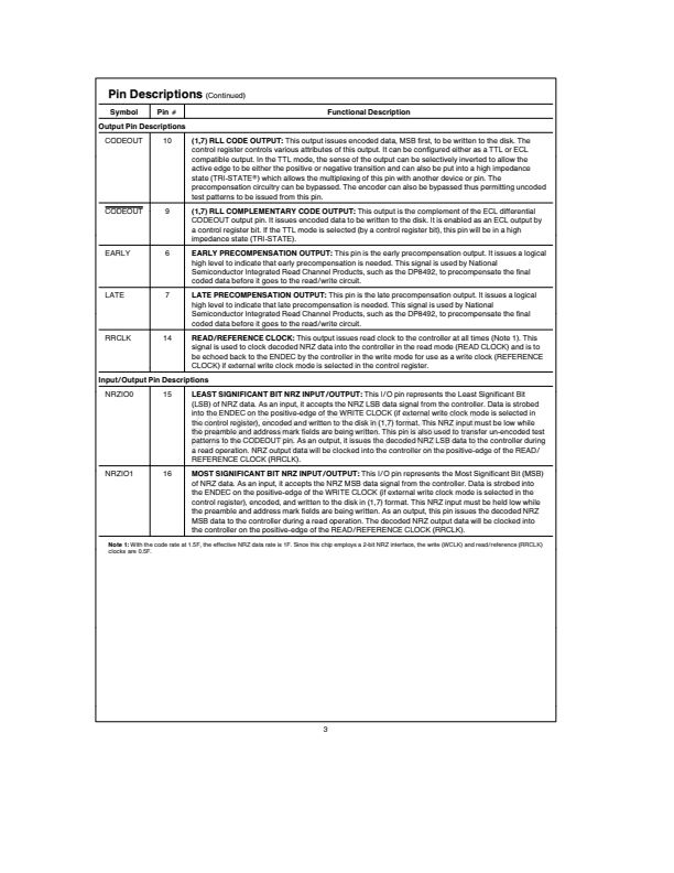 3
3
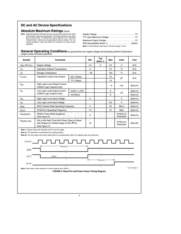 4
4
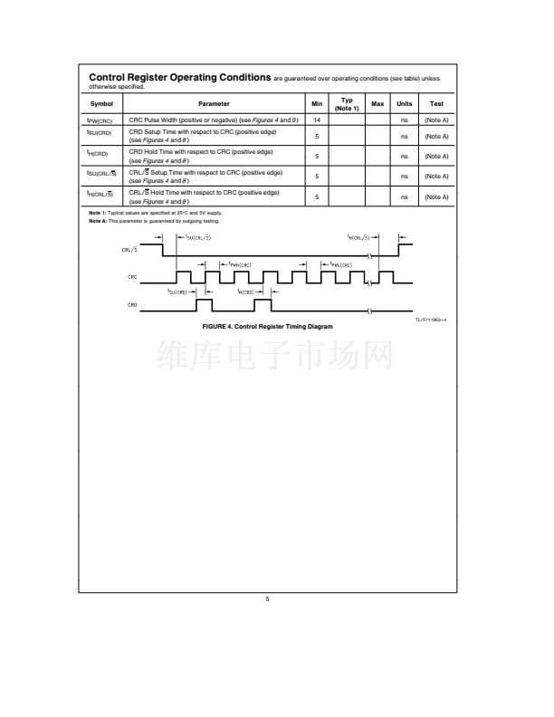 5
5
 6
6
 7
7
 8
8
 9
9
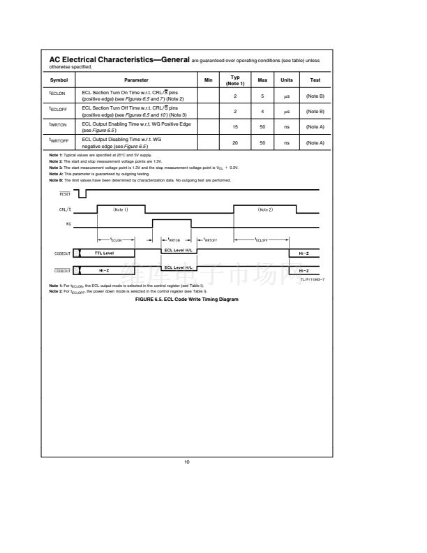 10
10
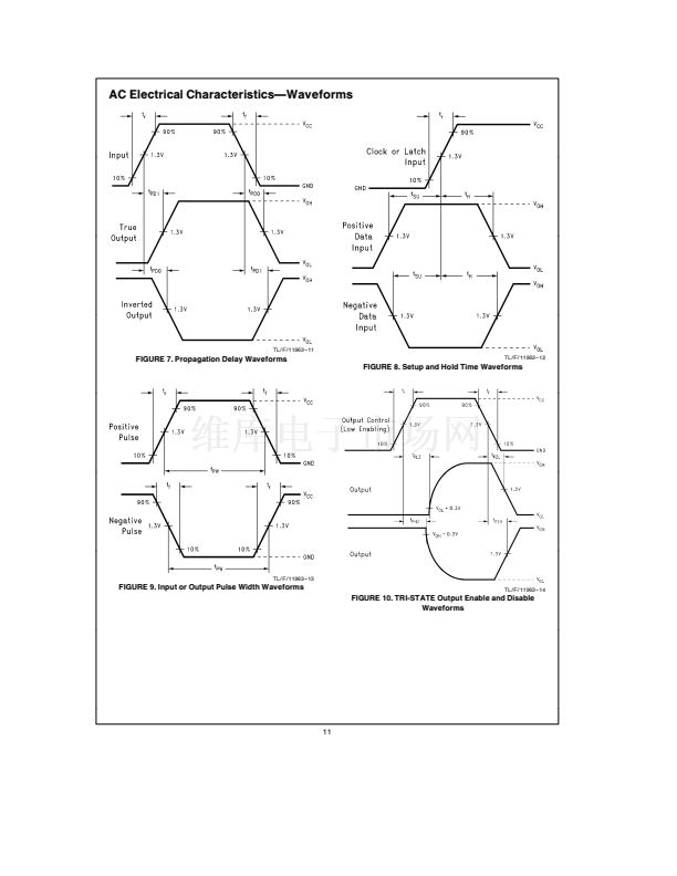 11
11
 12
12
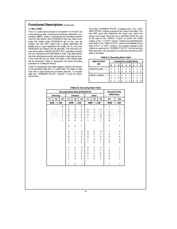 13
13
 14
14
 15
15
 16
16
