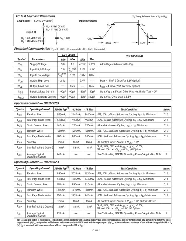
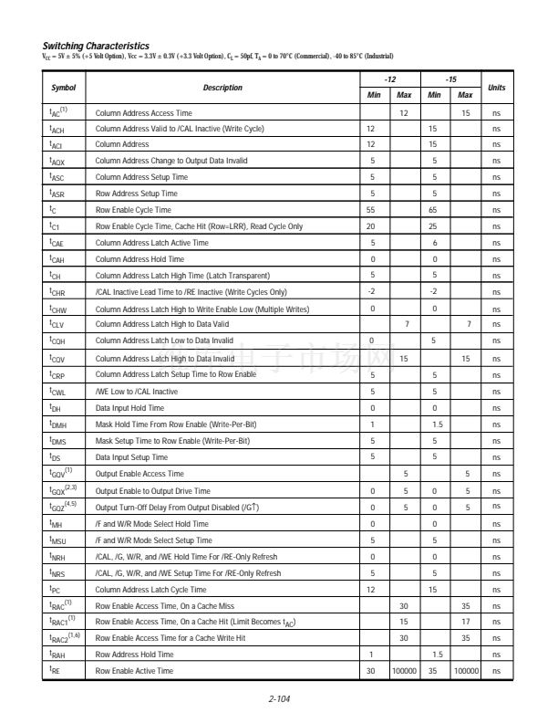
Enhanced
Features
Memory Systems Inc.
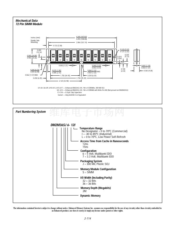
DM2M36SJ6/DM2M32SJ6 Multibank EDO
2Mbx36/2Mbx32 Enhanced DRAM SIMM
Product Specification
Architecture
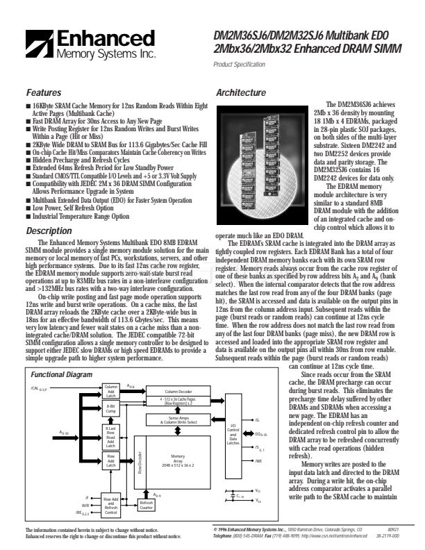
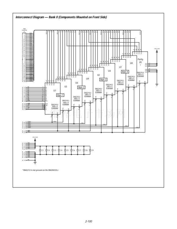
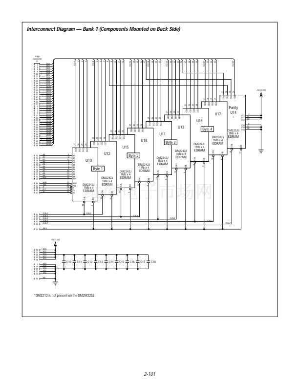
The DM2M36SJ6 achieves
2Mb x 36 density by mounting
18 1Mb x 4 EDRAMs, packaged
in 28-pin plastic SOJ packages,
on both sides of the multi-layer
substrate. Sixteen DM2242 and
two DM2252 devices provide
data and parity storage. The
DM2M32SJ6 contains 16
DM2242 devices for data only.
The EDRAM memory
module architecture is very
similar to a standard 8MB
DRAM module with the addition
of an integrated cache and on-
chip control which allows it to
s
16KByte SRAM Cache Memory for 12ns Random Reads Within Eight
Active Pages (Multibank Cache)
s
Fast DRAM Array for 30ns Access to Any New Page
s
Write Posting Register for 12ns Random Writes and Burst Writes
Within a Page (Hit or Miss)
s
2KByte Wide DRAM to SRAM Bus for 113.6 Gigabytes/Sec Cache Fill
s
On-chip Cache Hit/Miss Comparators Maintain Cache Coherency on Writes
s
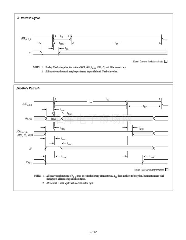
Hidden Precharge and Refresh Cycles
s
Extended 64ms Refresh Period for Low Standby Power
s
Standard CMOS/TTL Compatible I/O Levels and +5 or 3.3V Volt Supply
s
Compatibility with JEDEC 2M x 36 DRAM SIMM Configuration
Allows Performance Upgrade in System
s
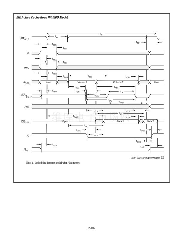
Multibank Extended Data Output (EDO) for Faster System Operation
s
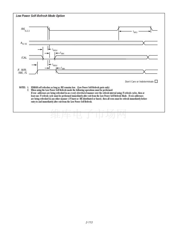
Low Power, Self Refresh Option
s
Industrial Temperature Range Option
operate much like an EDO DRAM.
The Enhanced Memory Systems Multibank EDO 8MB EDRAM
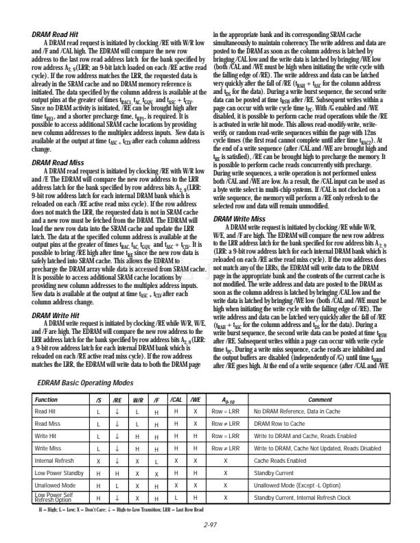
The EDRAM鈥檚 SRAM cache is integrated into the DRAM array as
SIMM module provides a single memory module solution for the main tightly coupled row registers. Each EDRAM Bank has a total of four
memory or local memory of fast PCs, workstations, servers, and other independent DRAM memory banks each with its own SRAM row
high performance systems. Due to its fast 12ns cache row register,
register. Memory reads always occur from the cache row register of
the EDRAM memory module supports zero-wait-state burst read
one of these banks as specified by row address bits A
2
and A
9
(bank
operations at up to 83MHz bus rates in a non-interleave configuration select). When the internal comparator detects that the row address
and >132MHz bus rates with a two-way interleave configuration.
matches the last row read from any of the four DRAM banks (page
On-chip write posting and fast page mode operation supports
hit), the SRAM is accessed and data is available on the output pins in
12ns write and burst write operations. On a cache miss, the fast
12ns from the column address input. Subsequent reads within the
DRAM array reloads the 2KByte cache over a 2KByte-wide bus in
page (burst reads or random reads) can continue at 12ns cycle
18ns for an effective bandwidth of 113.6 Gbytes/sec. This means
time. When the row address does not match the last row read from
very low latency and fewer wait states on a cache miss than a non-
any of the last four DRAM banks (page miss), the new DRAM row is
integrated cache/DRAM solution. The JEDEC compatible 72-bit
SIMM configuration allows a single memory controller to be designed to accessed and loaded into the appropriate SRAM row register and
support either JEDEC slow DRAMs or high speed EDRAMs to provide a data is available on the output pins all within 30ns from row enable.
Subsequent reads within the page (burst reads or random reads)
simple upgrade path to higher system performance.
can continue at 12ns cycle time.
Since reads occur from the SRAM
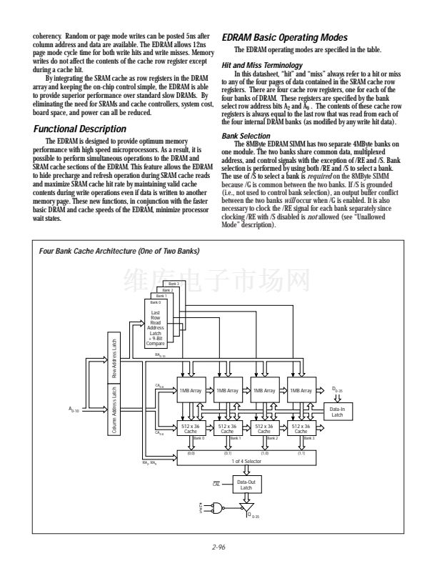
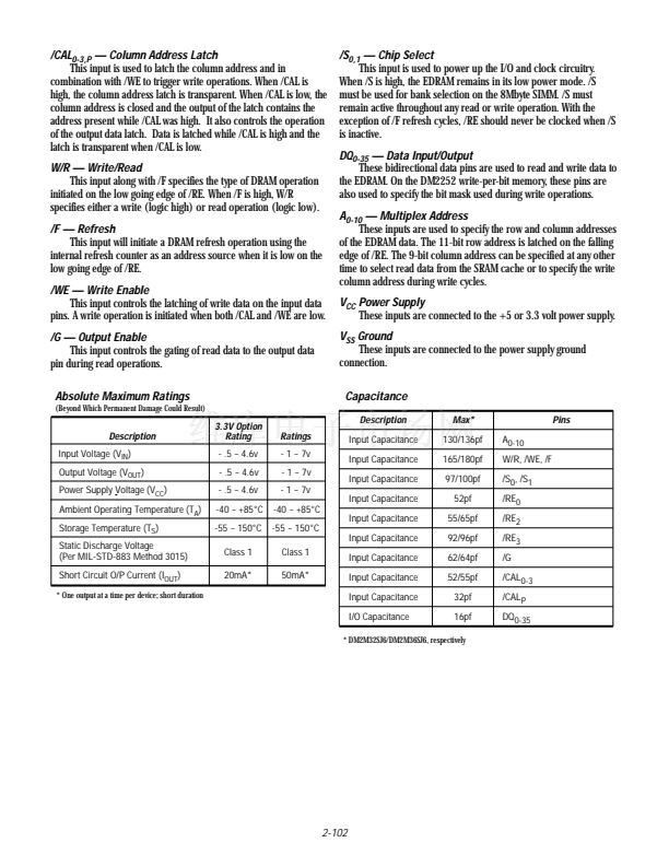
Functional Diagram
cache, the DRAM precharge can occur
A
0-8
Column
/CAL
0-3,P
Add
Column Decoder
during burst reads. This eliminates the
Latch
4 - 512 x 36 Cache Pages
precharge time delay suffered by other
(Row Registers) x 2
8-Bit
DRAMs and SDRAMs when accessing a
Comp
new page. The EDRAM has an
Sense Amps
/G
& Column Write Select
independent on-chip refresh counter and
I/O
8 Last
Control
A
0-10
dedicated refresh control pin to allow the
Row
DQ
0-35
and
Read
Data
DRAM array to be refreshed concurrently
Add
Latches
Latch
/S
with cache read operations (hidden
0, 1
Memory
Row
refresh).
Array
/WE
Add
2048 x 512 x 36 x 2
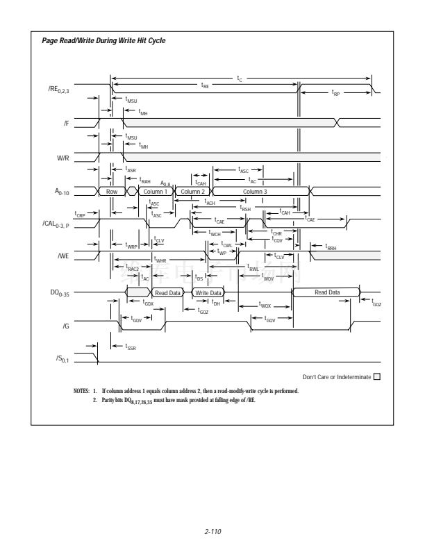
Memory writes are posted to the
Latch
input data latch and directed to the DRAM
array. During a write hit, the on-chip
address comparator activates a parallel
V
A
0-9
C
write path to the SRAM cache to maintain
/F
Row Add
V
Row Decoder
CC
1-18
Description
W/R
/RE
0,2,3
and
Refresh
Control
Refresh
Counter
SS
The information contained herein is subject to change without notice.
Enhanced reserves the right to change or discontinue this product without notice.
漏 1996 Enhanced Memory Systems Inc.,
1850 Ramtron Drive, Colorado Springs, CO
Telephone
(800) 545-DRAM;
Fax
(719) 488-9095; http://www.csn.net/ramtron/enhanced
80921
38-2119-000


 1
1
 2
2
 3
3
 4
4
 5
5
 6
6
 7
7
 8
8
 9
9
 10
10
 11
11
 12
12
 13
13
 14
14
 15
15
 16
16
 17
17
 18
18
 19
19
 20
20
