Semiconductor
April 1999
T
UCT
DUC
ROD TE PRO 747
TE P
OLE UBSTITU 00-442-7
OBS LE S
1-8
m
SIB lications arris.co
S
pp
A PO
@h
FOR Central A centapp
call r email:
o
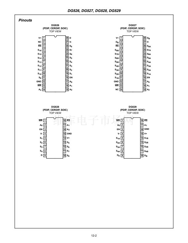
DG526, DG527,
DG528, DG529
Analog CMOS
Latchable Multiplexers
Features
鈥?Direct RESET
鈥?TTL and CMOS Compatible Address and Enable
Inputs
鈥?Maximum Power Supply Rating . . . . . . . . . . . . . . . . 44V
鈥?Break-Before-Make Switching
鈥?Alternate Source
Description
The DG526, DG527, DG528, and DG529 are CMOS
Monolithic 16-Channel/Dual 4-Channel Analog Multiplexers.
Each device has on-chip address and control latches to sim-
plify design in microprocessor based applications. The DG526
uses 4 address lines to control its 16 channels; the DG527,
DG528 both use 3 address lines to control their 8 channels;
and the DG529 uses 2 address lines to control its 4 channels.
The enable pin is used to enable the address latches during
the WR pulse. It can be hard wired to the logic supply if one of
the channels will always be used (except during a reset) or it
can be tied to address decoding circuitry for memory mapped
operation. The RS pin is used to clear all latches regardless of
the state of any other latch or control line. The WR pin is used
to transfer the state of the address control lines to their
latches, except during a reset or when EN is low.
A channel in the ON state conducts signals equally well in
both directions. In the OFF state each channel blocks volt-
ages up to the supply rails. The address inputs, WR, RS and
the enable input are TTL and CMOS compatible over the full
speci鏗乪d operation temperature range.
Applications
鈥?Data Acquisition Systems
鈥?Communication Systems
鈥?Automatic Test Equipment
鈥?Microprocessor Controlled Systemd
Part Number Information
PART
NUMBER
DG526AK
DG526AK/883B
DG526BK
DG526BY
DG526CJ
DG526CK
DG526CY
DG527AK
DG527AK/883B
DG527BK
DG527BY
DG527CJ
DG527CK
DG527CY
TEMP.
RANGE (
o
C)
-55 to 125
-55 to 125
-25 to 85
-25 to 85
0 to 70
0 to 70
0 to 70
-55 to 125
-55 to 125
-25 to 85
-25 to 85
0 to 70
0 to 70
0 to 70
PACKAGE
28 Ld CERDIP
28 Ld CERDIP
28 Ld CERDIP
28 Ld SOIC
28 Ld PDIP
28 Ld CERDIP
28 Ld SOIC
28 Ld CERDIP
28 Ld CERDIP
28 Ld CERDIP
28 Ld SOIC
28 Ld PDIP
28 Ld CERDIP
28 Ld SOIC
PKG. NO.
F28.6
F28.6
F28.6
M28.3
E28.6
F28.6
M28.3
F28.6
F28.6
F28.6
M28.3
E28.6
F28.6
M28.3
PART
NUMBER
DG528AK
DG528AK/883B
DG528BK
DG528BY
DG528CJ
DG528CK
DG528CY
DG529AK
DG529AK/883B
DG529BK
DG529BY
DG529CJ
DG529CK
DG529CY
TEMP.
RANGE (
o
C)
-55 to 125
-55 to 125
-25 to 85
-25 to 85
0 to 70
0 to 70
0 to 70
-55 to 125
-55 to 125
-25 to 85
-25 to 85
0 to 70
0 to 70
0 to 70
PACKAGE
18 Ld CERDIP
18 Ld CERDIP
18 Ld CERDIP
18 Ld SOIC
18 Ld PDIP
18 Ld CERDIP
18 Ld SOIC
18 Ld CERDIP
18 Ld CERDIP
18 Ld CERDIP
18 Ld SOIC
18 Ld PDIP
18 Ld CERDIP
18 Ld SOIC
PKG. NO.
F18.3
F18.3
F18.3
M18.3
E18.3
F18.3
M18.3
F18.3
F18.3
F18.3
M18.3
E18.3
F18.3
M18.3
CAUTION: These devices are sensitive to electrostatic discharge. Users should follow proper IC Handling Procedures.
Copyright
漏
Harris Corporation 1999
File Number
3139.2
12-1


 1
1
 2
2
 3
3
 4
4
 5
5
 6
6
 7
7
 8
8
 9
9
 10
10
 11
11
 12
12
 13
13
 14
14
 15
15
 16
16
