鈥?/div>
鹵0.5
LSB DNL
16-Bit Monotonic
鹵1
LSB INL
Low Noise: 12 nV/鈭欻z
Low Power: I
DD
= 2 碌A(chǔ)
+2.7 V to +5.5 V Analog Power Supply
2 mA Full-Scale Current
鹵20%,
with V
REF
= 10 V
50-MHz Serial Interface
0.5 碌s Settling Time
4-Quadrant Multiplying Reference
Reference Bandwidth: 10 MHz
鹵10
V Reference Input
Reference Dynamics: -105 THD
Tiny 8-Lead 3 x 3 mm SON and 3 x 5 mm
MSOP Packages
Industry-Standard Pin Configuration
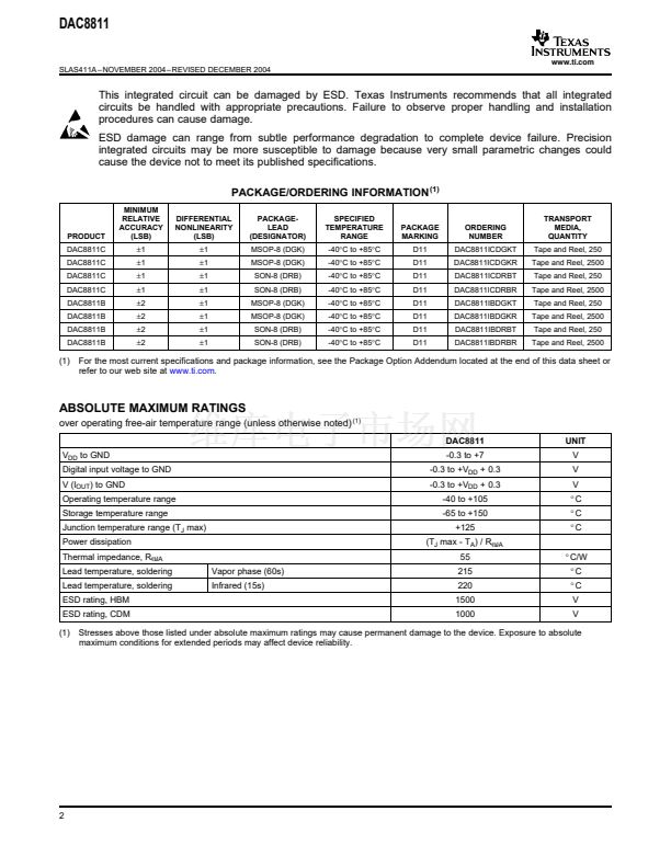
DESCRIPTION
The DAC8811 multiplying digital-to-analog converter
(DAC) is designed to operate from a single 2.7-V to
5.5-V supply.
The applied external reference input voltage V
REF
determines the full-scale output current. An internal
feedback resistor (R
FB
) provides temperature tracking
for the full-scale output when combined with an
external I-to-V precision amplifier.
A serial data interface offers high-speed, three-wire
microcontroller-compatible inputs using data-in (SDI),
clock (CLK), and chip-select (CS).
The DAC8811 is packaged in space-saving 8-lead
SON and MSOP packages.
DAC8811
V
DD
V
REF
D/A
Converter
16
R
FB
I
OUT
APPLICATIONS
Automatic Test Equipment
Instrumentation
Digitally Controlled Calibration
Industrial Control PLCs
CS
DAC
Register
16
CLK
SDI
Shift
Register
GND
Please be aware that an important notice concerning availability, standard warranty, and use in critical applications of Texas
Instruments semiconductor products and disclaimers thereto appears at the end of this data sheet.
PRODUCTION DATA information is current as of publication date.
Products conform to specifications per the terms of the Texas
Instruments standard warranty. Production processing does not
necessarily include testing of all parameters.
Copyright 漏 2004, Texas Instruments Incorporated


 1
1
 2
2
 3
3
 4
4
 5
5
 6
6
 7
7
 8
8
 9
9
 10
10
 11
11
 12
12
 13
13
 14
14
 15
15
