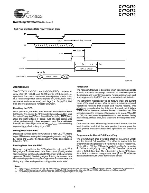
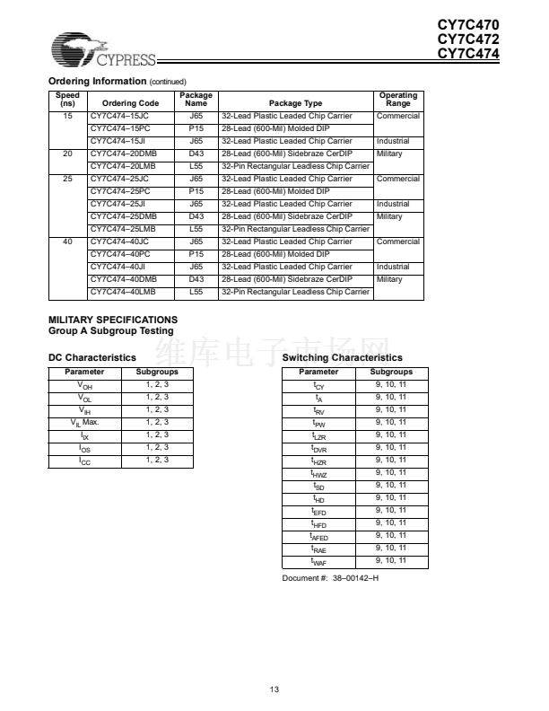
鈥?/div>
5V
鹵
10% supply
鈥?TTL compatible
鈥?Three-state outputs
鈥?Proprietary 0.8-micron CMOS technology
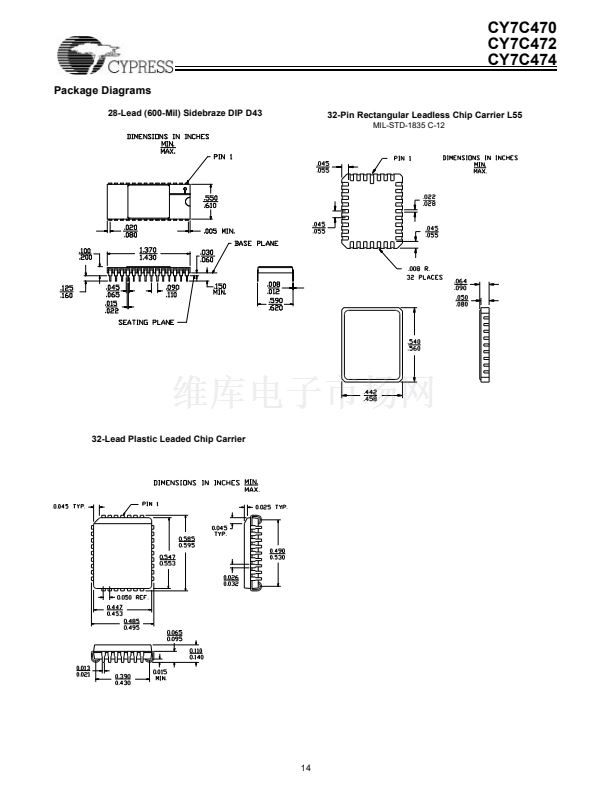
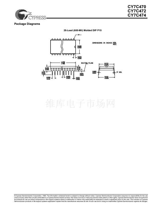
offered in 600-mil DIP, PLCC, and LCC packages. Each FIFO
memory is organized such that the data is read in the same
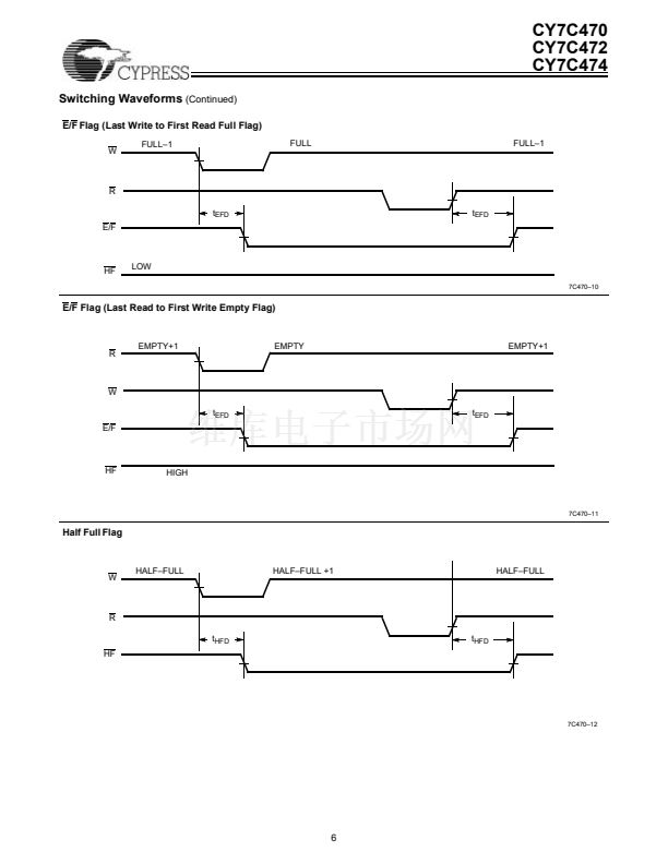
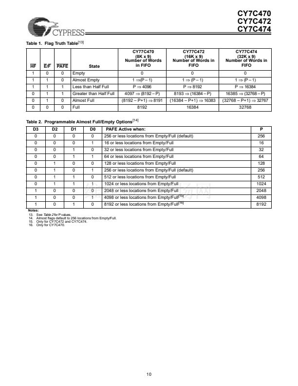
sequential order that it was written. Three status pins鈥擡mp-
ty/Full (E/F), Programmable Almost Full/Empty (PAFE), and
Half Full (HF)鈥攁re provided to the user. These pins are de-
coded to determine one of six states: Empty, Almost Empty,
Less than Half Full, Greater than Half Full, Almost Full, and
Full.
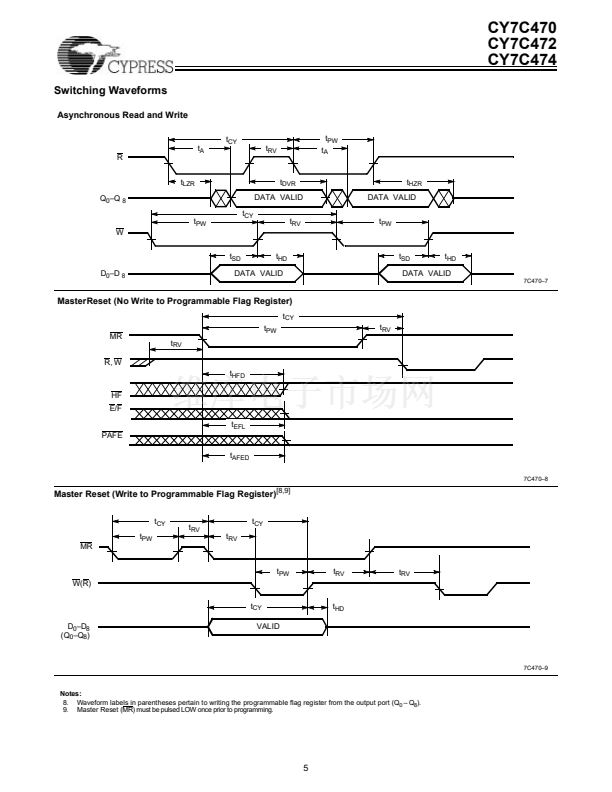
The read and write operations may be asynchronous; each
can occur at a rate of 33.3 MHz. The write operation occurs
when the write (W) signal goes LOW. Read occurs when read
(R) goes LOW. The nine data outputs go into a high-imped-
ance state when R is HIGH.
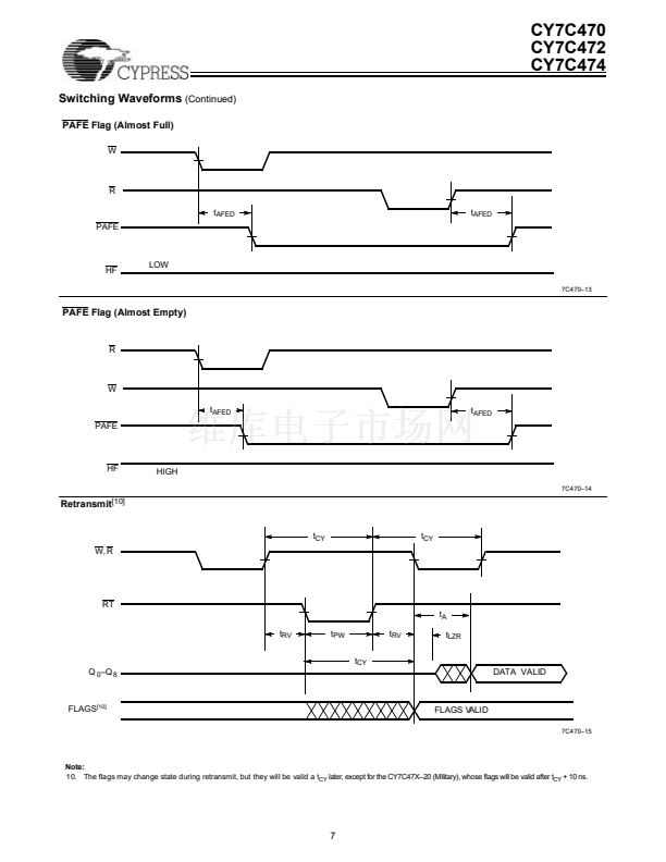
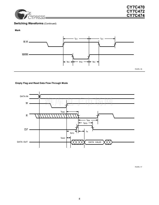
The user can store the value of the read pointer for retransmit
by using the MARK pin. A LOW on the retransmit (RT) input
causes the FIFO to resend data by resetting the read pointer
to the value stored in the mark pointer.
In the standalone and width expansion configurations, a LOW
on the retransmit (RT) input causes the FIFO to resend the
data. With the mark feature, retransmit can start from any word
in the FIFO.
The CYC47X series is fabricated using a proprietary 0.8-mi-
cron N-well CMOS technology. Input ESD protection is greater
than 2001V and latch-up is prevented by the use of reliable
layout techniques, guard rings, and a substrate bias generator.
Functional Description
The CYC47X FIFO series consists of high-speed, low-power,
first-in first-out (FIFO) memories with programmable flags and
retransmit mark. The CY7C470, CY7C472, and CY7C474 are
8K, 16K, and 32K words by 9 bits wide, respectively. They are
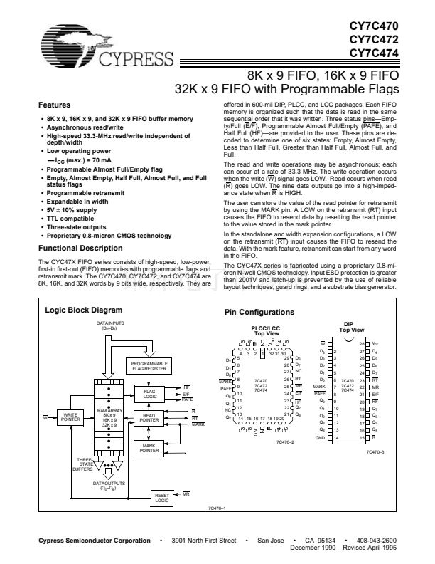
Logic Block Diagram
DATAINPUTS
(D
0
鈥揇
8
)
Pin Configurations
PLCC/LCC
Top View
W
4
PROGRAMMABLE
FLAG REGISTER
D
2
D
1
D
0
MARK
FLAG
LOGIC
HF
E/F
PAFE
R
RT
MARK
PAFE
Q
0
Q
1
NC
Q
2
5
6
7
8
9
10
11
12
7C470
7C472
7C474
3
2
1
32 31 30
29
28
27
26
25
24
23
22
D
8
D
6
D
7
NC
RT
MR
E/F
HF
Q
7
Q
6
D
3
D
2
D
1
D
0
MARK
PAFE
Q
0
Q
1
Q
2
Q
3
Q
8
GND
MARK
POINTER
7C470鈥?
1
2
3
4
5
6
7
8
9
10
11
12
13
14
7C470
7C472
7C474
DIP
Top View
28
27
26
25
24
23
22
21
20
19
18
17
16
15
V
cc
D
4
D
5
D
6
D
7
RT
MR
E/F
HF
Q
7
Q
6
Q
5
Q
4
R
W
WRITE
POINTER
RAM ARRAY
8K x 9
16K x 9
32K x 9
READ
POINTER
13
21
14 15 16 17 18 19 20
7C470鈥?
THREE鈥?/div>
STATE
BUFFERS
DATAOUTPUTS
(Q
0
鈥換
8
)
RESET
LOGIC
MR
7C470鈥?
Cypress Semiconductor Corporation
鈥?/div>
3901 North First Street
鈥?/div>
San Jose
鈥?CA 95134 鈥?/div>
408-943-2600
December 1990 鈥?Revised April 1995


 1
1
 2
2
 3
3
 4
4
 5
5
 6
6
 7
7
 8
8
 9
9
 10
10
 11
11
 12
12
 13
13
 14
14
 15
15
