鈥?/div>
Fast clock speed: 250, 200, and 167 MHz
Provide high-performance 3-1-1-1 access rate
Fast access time: 2.6, 3.0, and 3.4 ns
Optimal for depth expansion
Single 3.3V 鈥?% and +5% power supply V
DD
Separate V
DDQ
for 3.3V or 2.5V
Common data inputs and data outputs
Byte Write Enable and Global Write control
Chip enable for address pipeline
Address, data, and control registers
Internally self-timed Write Cycle
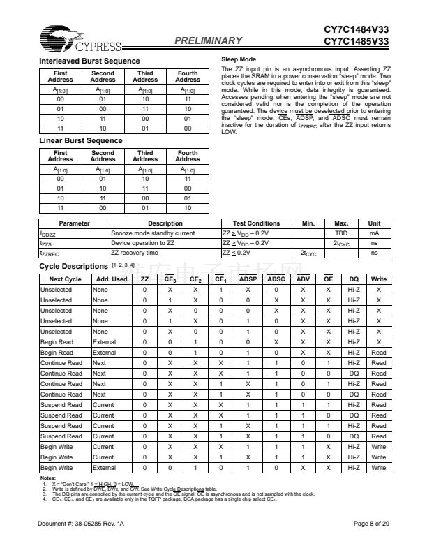
Burst control pins (interleaved or linear burst
sequence)
Automatic power-down for portable applications
High-density, high-speed packages
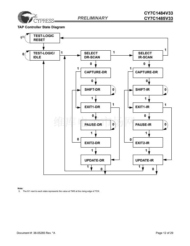
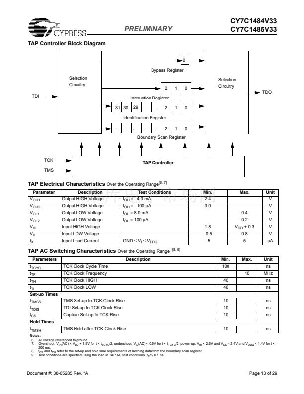
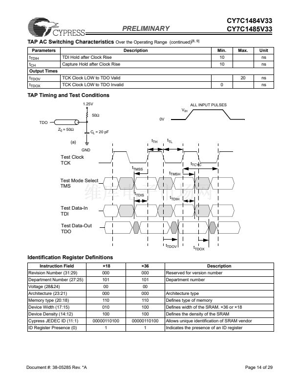
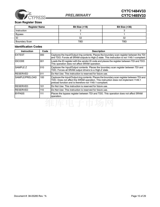
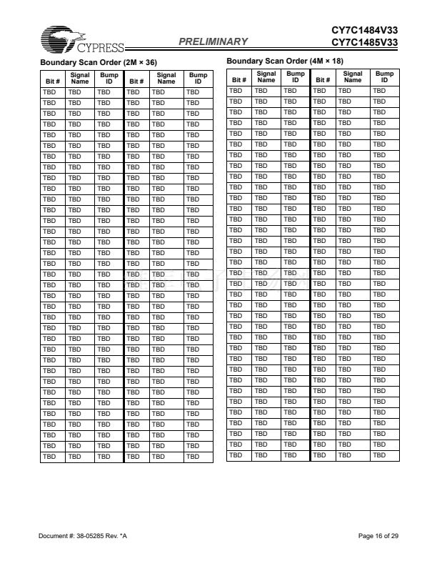
JTAG boundary scan for BGA packaging version
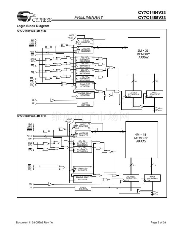
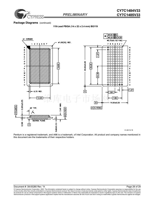
Available in 119-ball bump BGA and 100-pin TQFP
packages (CY7C1484V33 and CY7C1485V33).
165-ball FBGA will be offered on an opportunity basis.
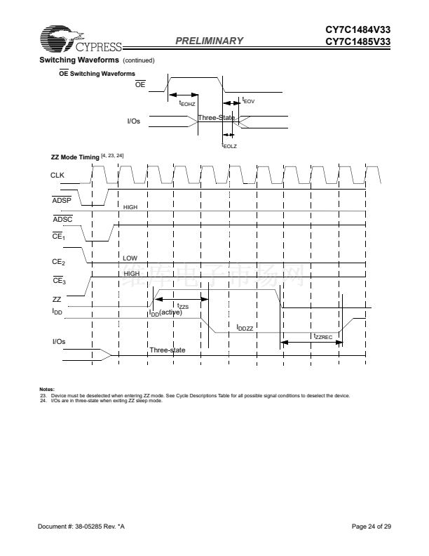
(Please contact Cypress sales or marketing)
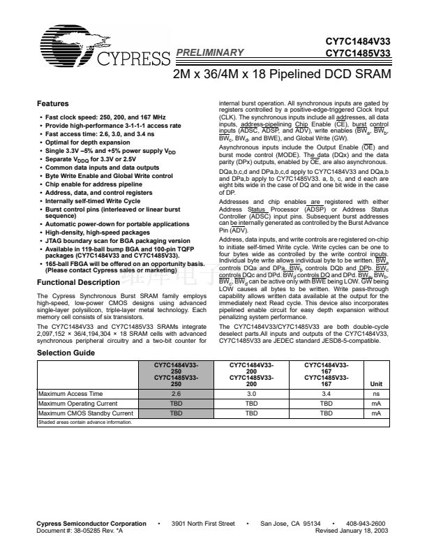
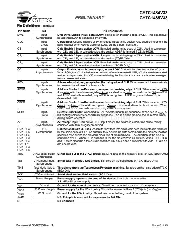
internal burst operation. All synchronous inputs are gated by
registers controlled by a positive-edge-triggered Clock Input
(CLK). The synchronous inputs include all addresses, all data
inputs, address-pipelining Chip Enable (CE), burst control
inputs (ADSC, ADSP, and ADV), write enables (BW
a
, BW
b
,
BW
c
, BW
d
, and BWE), and Global Write (GW).
Asynchronous inputs include the Output Enable (OE) and
burst mode control (MODE). The data (DQx) and the data
parity (DPx) outputs, enabled by OE, are also asynchronous.
DQa,b,c,d and DPa,b,c,d apply to CY7C1484V33 and DQa,b
and DPa,b apply to CY7C1485V33. a, b, c, and d each are
eight bits wide in the case of DQ and one bit wide in the case
of DP.
Addresses and chip enables are registered with either
Address Status Processor (ADSP) or Address Status
Controller (ADSC) input pins. Subsequent burst addresses
can be internally generated as controlled by the Burst Advance
Pin (ADV).
Address, data inputs, and write controls are registered on-chip
to initiate self-timed Write cycle. Write cycles can be one to
four bytes wide as controlled by the write control inputs.
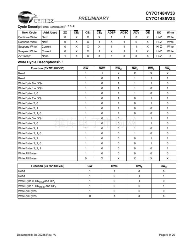
Individual byte write allows individual byte to be written. BW
a
controls DQa and DPa. BW
b
controls DQb and DPb. BW
c
controls DQc and DPd. BW
d
controls DQ and DPd. BW
a
, BW
b
,
BW
c
, BW
d
can be active only with BWE being LOW. GW being
LOW causes all bytes to be written. Write pass-through
capability allows written data available at the output for the
immediately next Read cycle. This device also incorporates
pipelined enable circuit for easy depth expansion without
penalizing system performance.
The CY7C1484V33/CY7C1485V33 are both double-cycle
deselect parts.All inputs and outputs of the CY7C1484V33,
CY7C1485V33 are JEDEC standard JESD8-5-compatible.
Functional Description
The Cypress Synchronous Burst SRAM family employs
high-speed, low-power CMOS designs using advanced
single-layer polysilicon, triple-layer metal technology. Each
memory cell consists of six transistors.
The CY7C1484V33 and CY7C1485V33 SRAMs integrate
2,097,152 脳 36/4,194,304 脳 18 SRAM cells with advanced
synchronous peripheral circuitry and a two-bit counter for
Selection Guide
CY7C1484V33-
250
CY7C1485V33-
250
Maximum Access Time
Maximum Operating Current
Maximum CMOS Standby Current
Shaded areas contain advance information.
CY7C1484V33-
200
CY7C1485V33-
200
3.0
TBD
TBD
CY7C1484V33-
167
CY7C1485V33-
167
3.4
TBD
TBD
Unit
ns
mA
mA
2.6
TBD
TBD
Cypress Semiconductor Corporation
Document #: 38-05285 Rev. *A
鈥?/div>
3901 North First Street
鈥?/div>
San Jose
,
CA 95134
鈥?/div>
408-943-2600
Revised January 18, 2003


 1
1
 2
2
 3
3
 4
4
 5
5
 6
6
 7
7
 8
8
 9
9
 10
10
 11
11
 12
12
 13
13
 14
14
 15
15
 16
16
 17
17
 18
18
 19
19
 20
20
 21
21
 22
22
 23
23
 24
24
 25
25
 26
26
 27
27
 28
28
 29
29
