錚?/div>
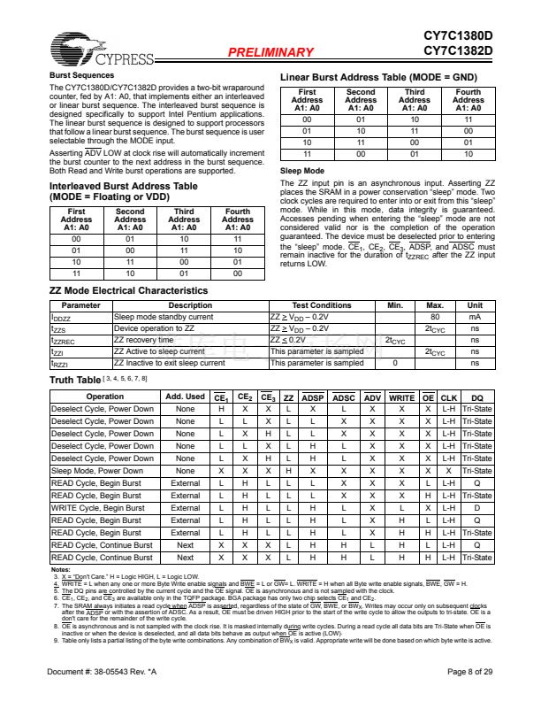
Pentium interleaved or linear burst sequences
Separate processor and controller address strobes
Synchronous self-timed writes
Asynchronous output enable
Single Cycle Chip Deselect
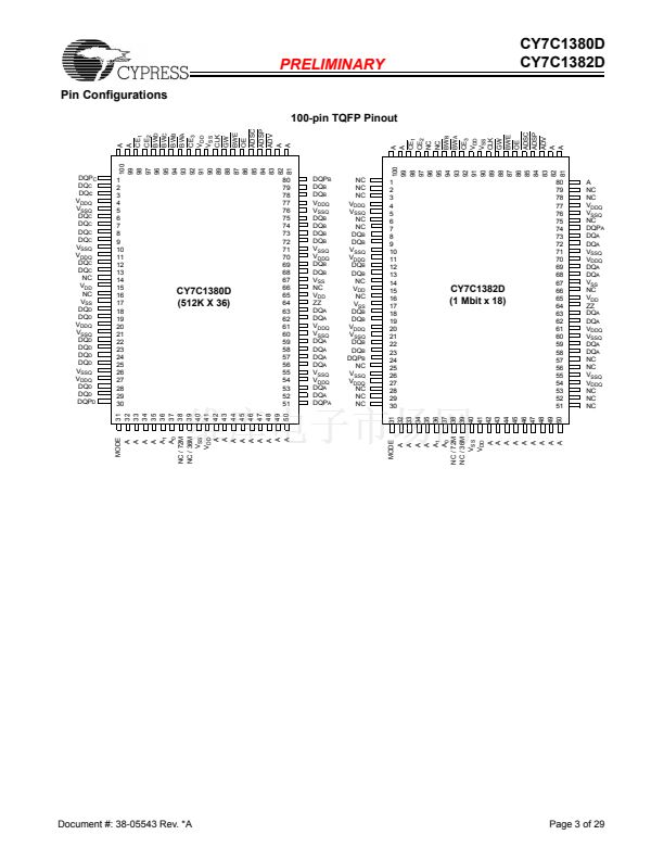
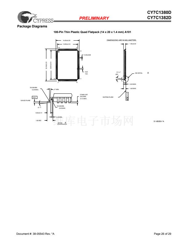
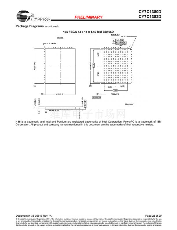
Offered in JEDEC-standard lead-free 100-pin TQFP,
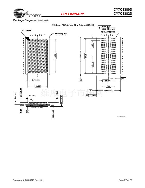
119-ball BGA and 165-Ball fBGA packages
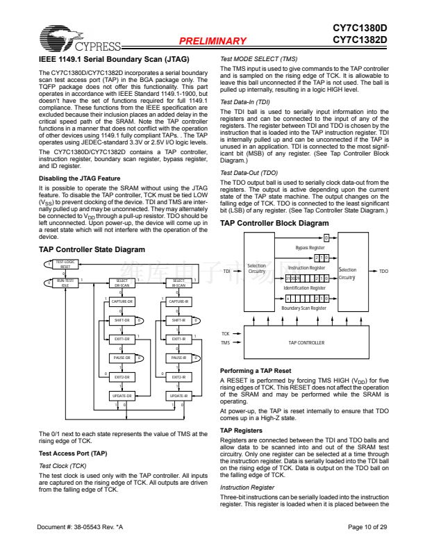
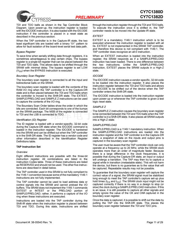
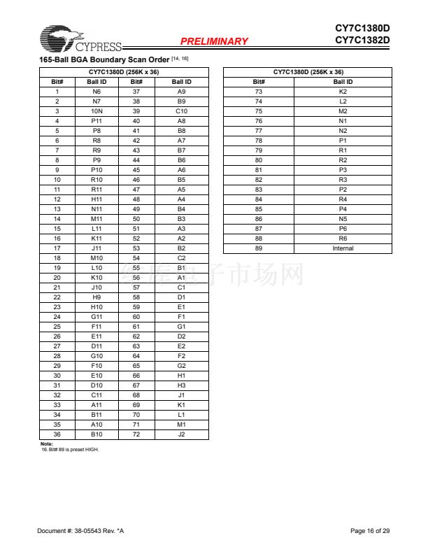
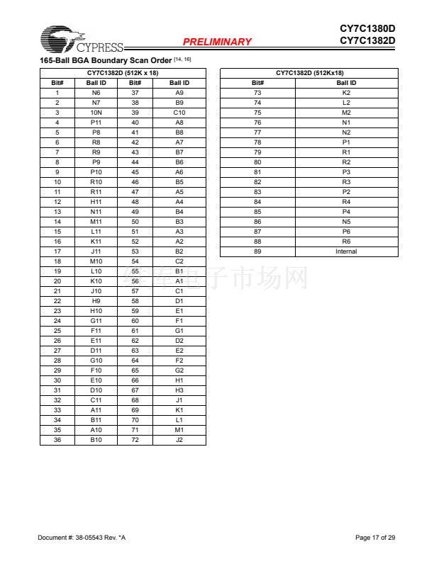
IEEE 1149.1 JTAG-Compatible Boundary Scan
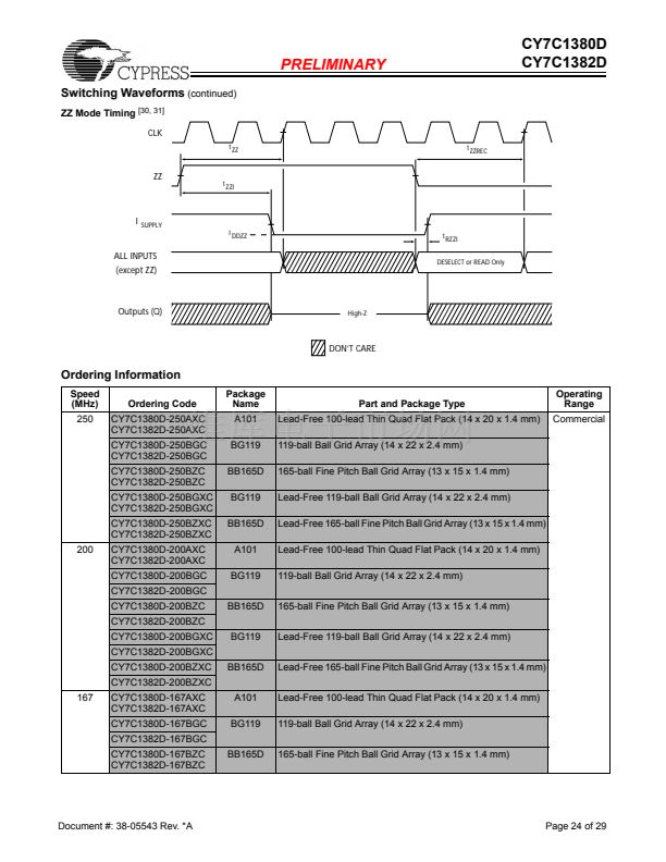
鈥淶Z鈥?Sleep Mode Option
Functional Description
[1]
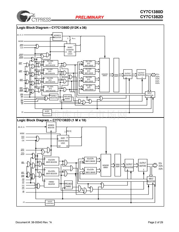
The CY7C1380D/CY7C1382D SRAM integrates 524,288 x 36
and 1,048,576 x 18 SRAM cells with advanced synchronous
peripheral circuitry and a two-bit counter for internal burst
operation. All synchronous inputs are gated by registers
controlled by a positive-edge-triggered Clock Input (CLK). The
synchronous inputs include all addresses, all data inputs,
address-pipelining Chip Enable (CE
1
), depth-expansion Chip
Enables (CE
2
and CE
3[2]
), Burst Control inputs (ADSC, ADSP,
and ADV), Write Enables (BW
X
, and BWE), and Global Write
(GW). Asynchronous inputs include the Output Enable (OE)
and the ZZ pin.
Addresses and chip enables are registered at rising edge of
clock when either Address Strobe Processor (ADSP) or
Address Strobe Controller (ADSC) are active. Subsequent
burst addresses can be internally generated as controlled by
the Advance pin (ADV).
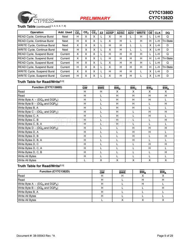
Address, data inputs, and write controls are registered on-chip
to initiate a self-timed Write cycle.This part supports Byte Write
operations (see Pin Descriptions and Truth Table for further
details). Write cycles can be one to two or four bytes wide as
controlled by the byte write control inputs. GW when active
LOW causes all bytes to be written.
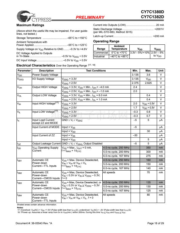
The CY7C1380D/CY7C1382D operates from a +3.3V core
power supply while all outputs may operate with either a +2.5
or +3.3V supply. All inputs and outputs are JEDEC-standard
JESD8-5-compatible.
鈥?/div>
鈥?/div>
鈥?/div>
鈥?/div>
鈥?/div>
鈥?/div>
鈥?/div>
鈥?/div>
鈥?/div>
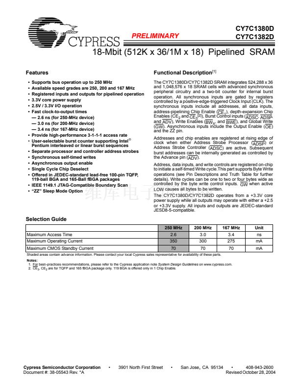
Selection Guide
250 MHz
Maximum Access Time
Maximum Operating Current
Maximum CMOS Standby Current
2.6
350
70
200 MHz
3.0
300
70
167 MHz
3.4
275
70
Unit
ns
mA
mA
Shaded areas contain advance information. Please contact your local Cypress sales representative for availability of these parts.
Notes:
1. For best鈥損ractices recommendations, please refer to the Cypress application note
System Design Guidelines
on www.cypress.com.
2. CE
3
, CE
2
are for TQFP and 165 fBGA package only. 119 BGA is offered only in 1 Chip Enable.
Cypress Semiconductor Corporation
Document #: 38-05543 Rev. *A
鈥?/div>
3901 North First Street
鈥?/div>
San Jose
,
CA 95134
鈥?/div>
408-943-2600
Revised October 28, 2004
CY7C1380D-167BGI相關型號PDF文件下載
-
型號
版本
描述
廠商
下載
-
英文版
16K x 8/9 Dual-Port Static RAM with Sem, Int, Busy
Cypress
-
英文版
32K x 8/9 Dual-Port Static RAM
Cypress
-
英文版
64K/128K x 8/9 Dual-Port Static RAM
CYPRESS
-
英文版
64K/128K x 8/9 Dual-Port Static RAM
CYPRESS [C...
-
英文版
64K/128K x 8/9 Dual-Port Static RAM
CYPRESS
-
英文版
64K/128K x 8/9 Dual-Port Static RAM
CYPRESS [C...
-
英文版
4K x 16/18 and 8K x 16/18 Dual-Port Static RAM with SEM, INT...
CYPRESS
-
英文版
4K x 16/18 and 8K x 16/18 Dual-Port Static RAM with SEM, INT...
CYPRESS [C...
-
英文版
4K x 16/18 and 8K x 16/18 Dual-Port Static RAM with Sem, Int...
Cypress
-
英文版
16K x 16/18 Dual-Port Static RAM
Cypress
-
英文版
32K/64K x 16/18 Dual-Port Static RAM
CYPRESS
-
英文版
32K/64K x 16/18 Dual-Port Static RAM
CYPRESS [C...
-
英文版
32K/64K x 16/18 Dual-Port Static RAM
CYPRESS
-
英文版
32K/64K x 16/18 Dual-Port Static RAM
CYPRESS [C...


 1
1
 2
2
 3
3
 4
4
 5
5
 6
6
 7
7
 8
8
 9
9
 10
10
 11
11
 12
12
 13
13
 14
14
 15
15
 16
16
 17
17
 18
18
 19
19
 20
20
 21
21
 22
22
 23
23
 24
24
 25
25
 26
26
 27
27
 28
28
 29
29
