鈥?/div>
Fast access times: 2.5 and 3.5 ns
Fast clock speed: 250, 225, 200, and 166 MHz
1.5 ns set-up time and 0.5 ns hold time
Fast OE access times: 2.5 ns and 3.5 ns
Optimal for depth expansion (one cycle chip deselect
to eliminate bus contention)
3.3V 鈥?% and +10% power supply
3.3V or 2.5V I/O supply
5V tolerant inputs except I/Os
Clamp diodes to V
SS
at all inputs and outputs
Common data inputs and data outputs
Byte Write Enable and Global Write control
Three chip enables for depth expansion and address
pipeline
Address, data, and control registers
Internally self-timed Write Cycle
Burst control pins (interleaved or linear burst se-
quence)
Automatic power-down for portable applications
JTAG boundary scan
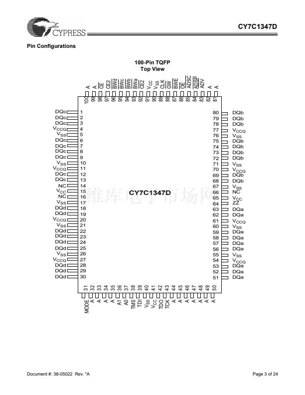
JEDEC standard pinout
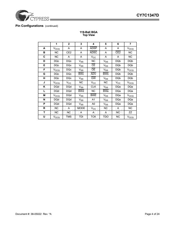
Low profile 119-lead, 14-mm x 22-mm BGA (Ball Grid
Array) and 100-pin TQFP packages
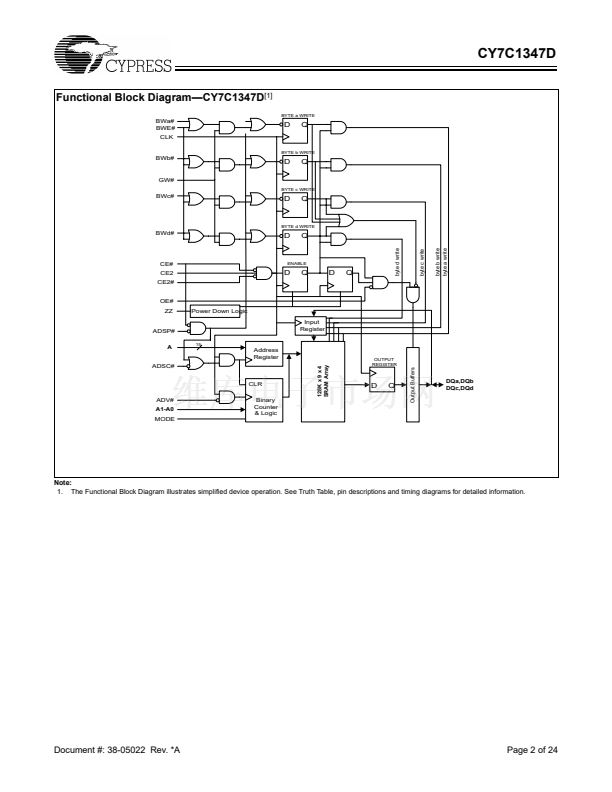
The CY7C1347D SRAM integrate 131,072 x 36 SRAM cells
with advanced synchronous peripheral circuitry and a 2-bit
counter for internal burst operation. All synchronous inputs are
gated by registers controlled by a positive-edge-triggered
clock input (CLK). The synchronous inputs include all address-
es, all data inputs, address-pipelining Chip Enable (CE),
depth-expansion Chip Enables (CE2 and CE2), Burst Control
Inputs (ADSC, ADSP, and ADV), Write Enables (BWa, BWb,
BWc, BWd, and BWE), and Global Write (GW).
Asynchronous inputs include the Output Enable (OE) and
Burst Mode Control (MODE). The data outputs (Q), enabled
by OE, are also asynchronous.
Addresses and chip enables are registered with either Ad-
dress Status Processor (ADSP) or Address Status Controller
(ADSC) input pins. Subsequent burst addresses can be inter-
nally generated as controlled by the Burst Advance pin (ADV).
Address, data inputs, and write controls are registered on-chip
to initiate self-timed Write cycle. Write cycles can be one to
four bytes wide as controlled by the write control inputs. Indi-
vidual byte write allows individual byte to be written. BWa con-
trols DQa. BWb controls DQb. BWc controls DQc. BWd con-
trols DQd. BWa, BWb, BWc, and BWd can be active only with
BWE being LOW. GW being LOW causes all bytes to be writ-
ten.
Four pins are used to implement JTAG test capabilities: Test
Mode Select (TMS), Test Data-in (TDI), Test Clock (TCK), and
Test Data-out (TDO). The JTAG circuitry is used to serially shift
data to and from the device. JTAG inputs use LVTTL/LVCMOS
levels to shift data during this testing mode of operation.
The CY7C1347D operates from a +3.3V power supply. All in-
puts and outputs are LVTTL compatible
Functional Description
This Cypress Synchronous Burst SRAM employs high-speed,
low-power CMOS designs using advanced triple-layer
polysilicon, double-layer metal technology. Each memory cell
consists of four transistors and two high-valued resistors.
Selection Guide
CY7C1347D-250
Maximum Access Time (ns)
Maximum Operating Current (mA)
Maximum CMOS Standby Current (mA)
2.5
450
10
CY7C1347D-225
2.5
400
10
CY7C1347D-200
2.5
360
10
CY7C1347D-166
3.5
300
10
Cypress Semiconductor Corporation
Document #: 38-05022 Rev. *A
鈥?/div>
3901 North First Street
鈥?/div>
San Jose
鈥?/div>
CA 95134 鈥?408-943-2600
Revised June 6, 2001


 1
1
 2
2
 3
3
 4
4
 5
5
 6
6
 7
7
 8
8
 9
9
 10
10
 11
11
 12
12
 13
13
 14
14
 15
15
 16
16
 17
17
 18
18
 19
19
 20
20
 21
21
 22
22
 23
23
 24
24
