CY7C1049BV33
512K x 8 Static RAM
1CY7C1049BV33
Features
鈥?High speed
鈥?t
AA
= 15 ns
鈥?Low active power
鈥?504 mW (max.)
鈥?Low CMOS standby power (Commercial L version)
鈥?1.8 mW (max.)
鈥?2.0V Data Retention (660
碌W
at 2.0V retention)
鈥?Automatic power-down when deselected
鈥?TTL-compatible inputs and outputs
鈥?Easy memory expansion with CE and OE features
expansion is provided by an active LOW Chip Enable (CE), an
active LOW Output Enable (OE), and three-state drivers. Writ-
ing to the device is accomplished by taking Chip Enable (CE)
and Write Enable (WE) inputs LOW. Data on the eight I/O pins
(I/O
0
through I/O
7
) is then written into the location specified on
the address pins (A
0
through A
18
).
Reading from the device is accomplished by taking Chip
Enable (CE) and Output Enable (OE) LOW while forcing Write
Enable (WE) HIGH. Under these conditions, the contents of
the memory location specified by the address pins will appear
on the I/O pins.
The eight input/output pins (I/O
0
through I/O
7
) are placed in a
high-impedance state when the device is deselected (CE
HIGH), the outputs are disabled (OE HIGH), or during a write
operation (CE LOW, and WE LOW).
The CY7C1049BV33 is available in a standard 400-mil-wide
36-pin SOJ and 44-pin TSOPII packages with center power
and ground (revolutionary) pinout.
Functional Description
The CY7C1049BV33 is a high-performance CMOS Static
RAM organized as 524,288 words by 8 bits. Easy memory
Logic Block Diagram
Pin Configuration
SOJ
Top View
TSOP II
Top View
NC
A
18
A
17
A
16
A
15
OE
I/O
7
I/O
6
GND
V
CC
I/O
5
I/O
4
A
14
A
13
A
12
A
11
A
10
NC
NC
NC
1
2
3
4
5
6
7
8
9
10
11
12
13
14
15
16
17
18
19
20
21
22
44
43
42
41
40
39
38
37
36
35
34
33
32
31
30
29
28
27
26
25
24
23
I/O
0
IN P U T B U FF E R
A
0
A
1
A
2
A
3
A
4
A
5
A
6
A
7
A
8
A
9
A
10
I/O
1
R OW DEC ODER
I/O
2
SENSE AM PS
5 12 K x 8
A R R AY
I/O
3
I/O
4
I/O
5
CE
WE
OE
C O LU M N
DECODER
POWER
DOW N
I/O
6
I/O
7
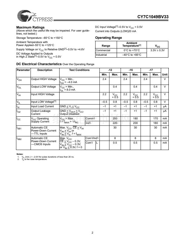
Selection Guide
-12
Maximum Access Time (ns)
Maximum Operating Current (mA) Comm鈥檒
Ind鈥檒
Maximum CMOS Standby
Current (mA)
Com鈥檒/Ind鈥檒
Com鈥檒
L
12
200
220
8
0.5
-15
15
180
200
8
0.5
-17
17
170
180
8
0.5
-20
20
160
170
8
0.5
-25
25
150
170
8
0.5
Cypress Semiconductor Corporation
A
11
A
12
A
13
A
14
A
15
A
16
A
17
A
18
A
0
A
1
A
2
A
3
A
4
CE
I/O
0
I/O
1
V
CC
GND
I/O
2
I/O 3
WE
A
5
A
6
A
7
A
8
A
9
1
2
3
4
5
6
7
8
9
10
11
12
13
14
15
16
17
18
36
35
34
33
32
31
30
29
28
27
26
25
24
23
22
21
20
19
NC
NC
NC
A
0
A
1
A
2
A
3
A
4
CE
I/O
0
I/O
1
V
CC
V
SS
I/O
2
I/O
3
WE
A
5
A
6
A
7
A
8
A
9
NC
NC
A
18
A
17
A
16
A
15
OE
I/O
7
I/O
6
V
SS
V
CC
I/O
5
I/O
4
A
14
A
13
A
12
A
11
A
10
NC
NC
NC
鈥?/div>
3901 North First Street
鈥?/div>
San Jose
鈥?/div>
CA 95134
鈥?/div>
408-943-2600
March 29, 2001


 1
1
 2
2
 3
3
 4
4
 5
5
 6
6
 7
7
 8
8
 9
9
