鈥?/div>
Available in 44-pin TSOP II and 400-mil SOJ
(BLE) is LOW, then data from I/O pins (I/O
1
through I/O
8
), is
written into the location specified on the address pins (A
0
through A
14
). If byte high enable (BHE) is LOW, then data from
I/O pins (I/O
9
through I/O
16
) is written into the location speci-
fied on the address pins (A
0
through A
14
).
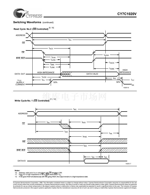
Reading from the device is accomplished by taking chip en-
able (CE) and output enable (OE) LOW while forcing the write
enable (WE) HIGH. If byte low enable (BLE) is LOW, then data
from the memory location specified by the address pins will
appear on I/O
1
to I/O
8
. If byte high enable (BHE) is LOW, then
data from memory will appear on I/O
9
to I/O
16
. See the truth
table at the back of this datasheet for a complete description
of read and write modes.
The input/output pins (I/O
1
through I/O
16
) are placed in a
high-impedance state when the device is deselected (CE
HIGH), the outputs are disabled (OE HIGH), the BHE and BLE
are disabled (BHE, BLE HIGH), or during a write operation (CE
LOW, and WE LOW).
The CY7C1020V is available in standard 44-pin TSOP type II
and 400-mil-wide SOJ packages.
Functional Description
The CY7C1020V is a high-performance CMOS static RAM or-
ganized as 32,768 words by 16 bits. This device has an auto-
matic power-down feature that significantly reduces power
consumption when deselected.
Writing to the device is accomplished by taking chip enable
(CE) and write enable (WE) inputs LOW. If byte low enable
Logic Block Diagram
DATA IN DRIVERS
Pin Configuration
SOJ / TSOP II
Top View
NC
A
14
A
13
A
12
A
11
CE
I/O
1
I/O
2
I/O
3
I/O
4
V
CC
V
SS
I/O
5
I/O
6
I/O
7
I/O
8
WE
A
10
A
9
A
8
A
7
NC
1
2
3
4
5
6
7
8
9
10
11
12
13
14
15
16
17
18
19
20
21
22
44
43
42
41
40
39
38
37
36
35
34
33
32
31
30
29
28
27
26
25
24
23
A
6
A
5
A
4
A
3
A
2
A
1
A
0
32K x 16
RAM Array
I/O
1
鈥?I/O
8
I/O
9
鈥?I/O
16
COLUMN DECODER
BHE
WE
CE
OE
BLE
1020V-1
A
0
A
1
A
2
OE
BHE
BLE
I/O
16
I/O
15
I/O
14
I/O
13
V
SS
V
CC
I/O
12
I/O
11
I/O
10
I/O
9
NC
A
3
A
4
A
5
A
6
NC
ROW DECODER
A
7
A
8
A
9
A
10
A
11
A
12
A
13
A
14
SENSE AMPS
1020V-2
Selection Guide
7C1020V-10
Maximum Access Time (ns)
Maximum Operating Current (mA)
L
Maximum CMOS Standby Current (mA)
L
10
130
100
1
0.1
7C1020V-12
12
120
90
1
0.1
7C1020V-15
15
110
80
1
0.1
7C1020V-20
20
100
70
1
0.1
Cypress Semiconductor Corporation
鈥?/div>
3901 North First Street
鈥?/div>
San Jose
鈥?/div>
CA 95134 鈥?/div>
408-943-2600
October 1996 - Revised April 13, 1998


 1
1
 2
2
 3
3
 4
4
 5
5
 6
6
 7
7
 8
8
 9
9
 10
10
 11
11
 12
12
 13
13
