CY54FCT841T, CY74FCT841T
10-BIT LATCHES
WITH 3-STATE OUTPUTS
SCCS035A 鈥?SEPTEMBER 1994 鈥?REVISED OCTOBER 2001
D
D
D
D
D
D
D
D
D
D
D
D
Function, Pinout, and Drive Compatible
With FCT, F, and AM29841 Logic
Reduced V
OH
(Typically = 3.3 V) Versions of
Equivalent FCT Functions
Edge-Rate Control Circuitry for
Significantly Improved Noise
Characteristics
I
off
Supports Partial-Power-Down Mode
Operation
Matched Rise and Fall Times
ESD Protection Exceeds JESD 22
鈥?2000-V Human-Body Model (A114-A)
鈥?200-V Machine Model (A115-A)
鈥?1000-V Charged-Device Model (C101)
Fully Compatible With TTL Input and
Output Logic Levels
High-Speed Parallel Latches
Buffered Common Latch-Enable Input
3-State Outputs
CY54FCT841T
鈥?32-mA Output Sink Current
鈥?12-mA Output Source Current
CY74FCT841T
鈥?64-mA Output Sink Current
鈥?32-mA Output Source Current
CY54FCT841T . . . D PACKAGE
CY74FCT841T . . . P, Q, OR SO PACKAGE
(TOP VIEW)
OE
D
0
D
1
D
2
D
3
D
4
D
5
D
6
D
7
D
8
D
9
GND
1
2
3
4
5
6
7
8
9
10
11
12
24
23
22
21
20
19
18
17
16
15
14
13
V
CC
Y
0
Y
1
Y
2
Y
3
Y
4
Y
5
Y
6
Y
7
Y
8
Y
9
LE
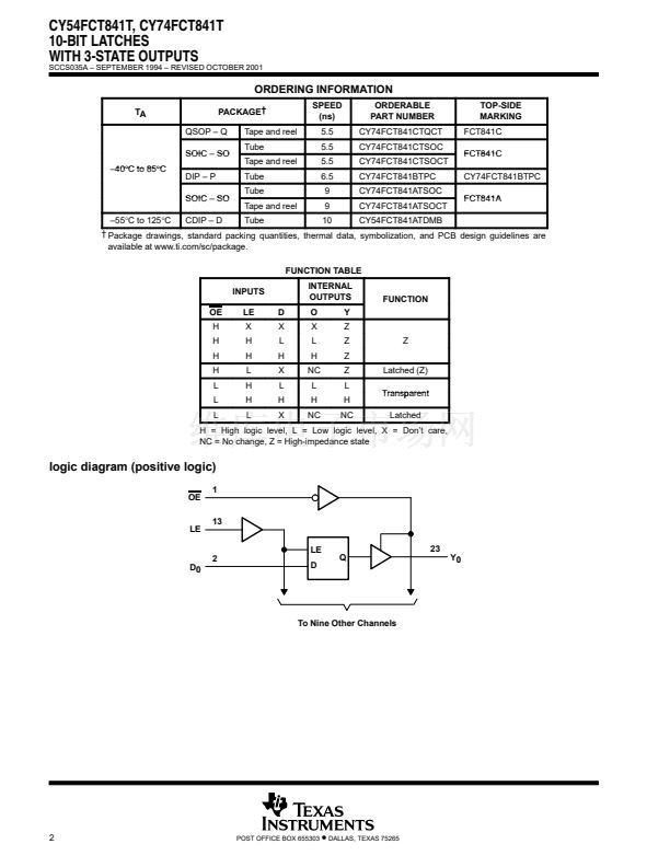
description
The 鈥橣CT841T bus-interface latches are designed to eliminate additional packages required to buffer existing
latches and provide additional data width for wider address/data paths or buses carrying parity. The 鈥橣CT841T
devices are buffered 10-bit-wide versions of the FCT373 function.
The 鈥橣CT841T devices鈥?high-performance interface is designed for high-capacitance-load drive capability, while
providing low-capacitance bus loading at both inputs and outputs. Outputs are designed for low-capacitance
bus loading in the high-impedance state.
These devices are fully specified for partial-power-down applications using I
off
. The I
off
circuitry disables the
outputs, preventing damaging current backflow through the device when it is powered down.
PIN DESCRIPTION
NAME
D
LE
Y
OE
I/O
I
I
O
I
Latch data inputs
Latch-enable input. The latches are transparent when LE is high.
Input data is latched on the high-to-low transition.
3-state latch outputs
Output-enable control. When OE is low, the outputs are enabled.
When OE is high, the outputs are in the high-impedance (off) state.
DESCRIPTION
Please be aware that an important notice concerning availability, standard warranty, and use in critical applications of
Texas Instruments semiconductor products and disclaimers thereto appears at the end of this data sheet.
Copyright
錚?/div>
2001, Texas Instruments Incorporated
On products compliant to MIL-PRF-38535, all parameters are tested
unless otherwise noted. On all other products, production
processing does not necessarily include testing of all parameters.
PRODUCTION DATA information is current as of publication date.
Products conform to specifications per the terms of Texas Instruments
standard warranty. Production processing does not necessarily include
testing of all parameters.
POST OFFICE BOX 655303
鈥?/div>
DALLAS, TEXAS 75265
1


 1
1
 2
2
 3
3
 4
4
 5
5
 6
6
 7
7
 8
8
