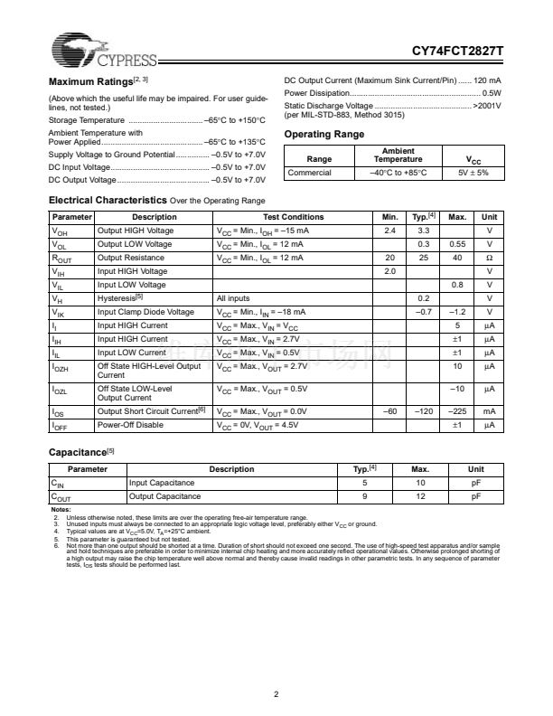
鈥?FCT-C speed at 5.0 ns max. (Com鈥檒),
FCT-A speed at 8.0 ns max. (Com鈥檒)
鈥?/div>
25鈩?output series resistors to reduce transmission line
reflection noise
鈥?Reduced V
OH
(typically = 3.3V) versions of equivalent
FCT functions
鈥?Edge-rate control circuitry for significantly improved
noise characteristics
鈥?Power-off disable feature
鈥?ESD > 2000V
鈥?Matched rise and fall times
鈥?Fully compatible with TTL input and output logic levels
鈥?Extended commercial temp. range of 鈥?0擄C to +85擄C
鈥?Sink current
Source current
12 mA
15 mA
Functional Description
The FCT2827T 10-bit bus driver provides high-performance
bus interface buffering for wide data/address paths or buses
carrying parity. This 10-bit buffer has NAND-ed output enables for
maximum control flexibility. The FCT2827T is designed for
high-capacitance load drive capability, while providing low-capaci-
tance bus loading at both inputs and outputs. All inputs have clamp
diodes and all outputs are designed for low-capacitance bus load-
ing in the high impedance state. On-chip termination resistors have
been added to the outputs to reduce system noise caused by re-
flections. The FCT2827T can be used to replace the FCT827T to
reduce noise in an existing design.
The outputs are designed with a power-off disable feature to
allow for live insertion of boards.
Logic Block Diagram
Pin Configurations
SOIC/QSOP
Top View
Y
0
Y
1
Y
2
Y
3
Y
4
Y
5
Y
6
Y
7
Y
8
Y
9
OE
1
D
0
D
1
D
2
D
3
D
4
D
5
D
6
D
7
D
8
D
9
GND
1
2
3
4
5
6
7
8
9
10
11
12
24
23
22
21
20
19
18
17
16
15
14
13
V
CC
Y
0
Y
1
Y
2
Y
3
Y
4
Y
5
Y
6
Y
7
Y
8
Y
9
OE
2
D
0
D
1
D
2
D
3
D
4
D
5
D
6
D
7
D
8
D
9
OE
1
OE
2
FCT2827T
鈥?
FCT2827T
鈥?
Function Table
[1]
Inputs
OE
1
L
L
H
X
OE
2
L
L
X
H
D
L
H
X
X
Outputs
Y
L
H
Z
Z
Function
Transparent
Three-State
Note:
1. H = HIGH Voltage Level. L = LOW Voltage Level. X = Don鈥檛 Care.
Cypress Semiconductor Corporation
鈥?/div>
3901 North First Street
鈥?/div>
San Jose
鈥?/div>
CA 95134 鈥?/div>
408-943-2600
May 1994 鈥?Revised October 1996


 1
1
 2
2
 3
3
 4
4
 5
5
