Data sheet acquired from Cypress Semiconductor Corporation.
Data sheet modi鏗乪d to remove devices not offered.
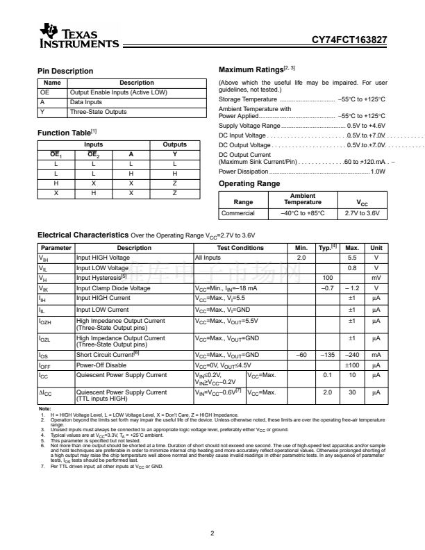
CY74FCT163827
SCCS049 - March 1997 - Revised March 2000
20-Bit Buffer
Functional Description
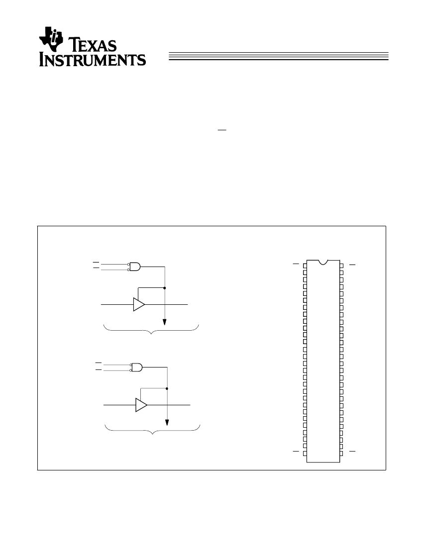
The CY74FCT163827 is a 20-bit buffer/line driver that provides
high-performance bus interface buffering for wide data/address
paths or buses carrying parity. It can be used as a single 20-bit
buffer or two 10-bit buffers. Each 10-bit buffer has a pair of NANDed
OE for increased flexibility.
The CY74FCT163827 has 24-mA balanced output drivers
with current limiting resistors in the outputs. This reduces the
need for external terminating resistors and provides for
minimal undershoot and reduced ground bounce. The inputs
and outputs were designed to be capable of being driven by
5.0V buses, allowing its use in mixed voltage systems as a
translator. The outputs are also designed with a power-off
disable feature enabling its use in applications requiring live
insertion.
Features
鈥?Low power, pin-compatible replacement for LCX and
LPT families
鈥?5V tolerant inputs and outputs
鈥?24 mA & 6 mA balanced drive outputs
鈥?Power-off disable outputs permits live insertion
鈥?Edge-rate control circuitry for reduced noise
鈥?FCT-C speed at 4.1 ns
鈥?Latch-up performance exceeds JEDEC standard no. 17
鈥?Typical output skew < 250 ps
鈥?Industrial temperature range of 鈥?0藲C to +85藲C
鈥?TSSOP (19.6-mil pitch) or SSOP (25-mil pitch)
鈥?Typical
V
olp
(ground bounce) performance exceeds Mil
Std 883D
鈥?V
CC
= 2.7V to 3.6V
鈥?ESD (HBM) > 2000V
Logic Block Diagrams CY74FCT163827
Pin Configuration
SSOP/TSSOP
Top View
1
OE
1
1
OE
2
1
OE
1
1
Y
1
1
Y
2
1
2
3
4
5
6
7
8
9
10
11
12
13
14
15
16
17
18
19
20
21
22
23
24
25
26
27
28
56
55
54
53
52
51
50
49
48
47
46
45
44
43
42
41
40
39
38
37
36
35
34
33
32
31
30
29
1
OE
2
1
A
1
1
A
2
GND
1
Y
3
1
A
1
1
Y
1
1
Y
4
GND
1
A
3
1
A
4
V
CC
1
Y
5
1
Y
6
1
Y
7
V
CC
1
A
5
1
A
6
1
A
7
TO 9 OTHER CHANNELS
FCT163827-1
GND
1
Y
8
1
Y
9
1
Y
10
GND
1
A
8
1
A
9
1
A
10
2
A
1
2
A
2
2
A
3
2
OE
1
2
OE
2
2
Y
1
2
Y
2
2
Y
3
GND
2
Y
4
2
Y
5
2
A
1
2
Y
1
2
Y
6
GND
2
A
4
2
A
5
2
A
6
V
CC
2
Y
7
2
Y
8
V
CC
2
A
7
2
A
8
GND
TO 9 OTHER CHANNELS
FCT163827-2
2
Y
9
2
Y
10
2
OE
1
GND
2
A
9
2
A
10
2
OE
2
Copyright
漏
2000, Texas Instruments Incorporated


 1
1
 2
2
 3
3
 4
4
 5
5
 6
6
