1CY74FCT162652T
Data sheet acquired from Cypress Semiconductor Corporation.
Data sheet modi鏗乪d to remove devices not offered.
CY74FCT16652T
CY74FCT162652T
SCCS061 - July 1994 - Revised March 2000
16-Bit Registered Transceivers
Functional Description
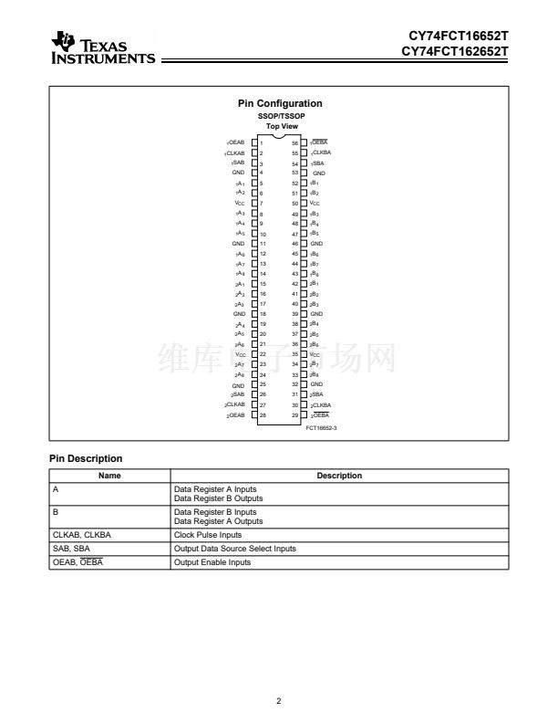
These 16-bit, high-speed, low-power, registered transceivers
that are organized as two independent 8-bit bus transceivers
with three-state D-type registers and control circuitry arranged
for multiplexed transmission of data directly from the input bus
or from the internal storage registers. OEAB and OEBA control
pins are provided to control the transceiver functions. SAB and
SBA control pins are provided to select either real-time or
stored data transfer.
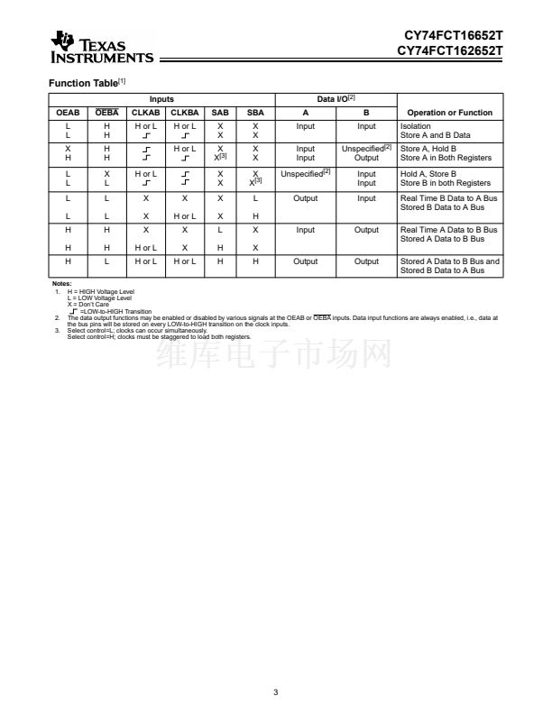
Data on the A or B data bus, or both, can be stored in the
internal D 鏗俰p-鏗俹ps by LOW-to-HIGH transitions at the
appropriate clock pins (CLKAB or CLKBA), regardless of the
select or enable control pins. When SAB and SBA are in the
real-time transfer mode, it is also possible to store data without
using the internal D-type 鏗俰p-鏗俹ps by simultaneously enabling
OEAB and OEBA. In this con鏗乬uration, each output reinforces
its input. Thus, when all other data sources to the two sets of
bus lines are at high impedance, each set of bus lines will
remain at its last state. The output buffers are designed with a
power-off disable feature that allows live insertion of boards.
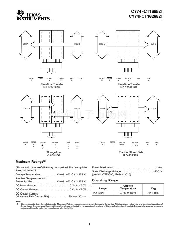
The CY74FCT16652T is ideally suited for driving
high-capacitance loads and low-impedance backplanes.
The CY74FCT162652T has 24-mA balanced output drivers
with current-limiting resistors in the outputs. This reduces the
need for external terminating resistors and provides for
minimal undershoot and reduced ground bounce. The
CY74FCT162652T is ideal for driving transmission lines.
Features
鈥?FCT-E speed at 3.8 ns
鈥?Power-off disable outputs permits live insertion
鈥?Edge-rate control circuitry for signi鏗乧antly improved
noise characteristics
鈥?Typical output skew < 250 ps
鈥?ESD > 2000V
鈥?TSSOP (19.6-mil pitch) and SSOP (25-mil pitch)
packages
鈥?Industrial temperature range of
鈭?0藲C
to +85藲C
鈥?V
CC
= 5V
鹵
10%
CY74FCT16652T Features:
鈥?64 mA sink current, 32 mA source current
鈥?Typical V
OLP
(ground bounce) <1.0V at V
CC
= 5V,
T
A
= 25藲C
CY74FCT162652T Features:
鈥?Balanced 24 mA output drivers
鈥?Reduced system switching noise
鈥?Typical V
OLP
(ground bounce) <0.6V at V
CC
= 5V,
T
A
= 25藲C
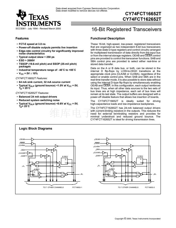
Logic Block Diagrams
1
OEAB
1
OEBA
1
CLKBA
1
SBA
1
CLKAB
1
SAB
2
OEAB
2
OEBA
2
CLKBA
2
SBA
2
CLKAB
B REG
D
C
2
SAB
B REG
D
C
1
A
1
2
A
1
A REG
D
C
1
B
1
A REG
D
C
2
B
1
TO 7 OTHER CHANNELS
FCT16652-1
TO 7 OTHER CHANNELS
FCT16652-2
Copyright
漏
2000, Texas Instruments Incorporated


 1
1
 2
2
 3
3
 4
4
 5
5
 6
6
 7
7
 8
8
 9
9
 10
10
