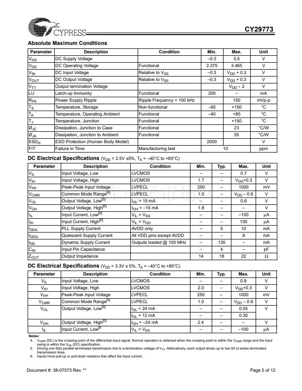
Spread Aware鈩?/div>
Output enable/disable
Pin-compatible with MPC9773 and MPC973
Industrial temperature range: 鈥?0擄C to +85擄C
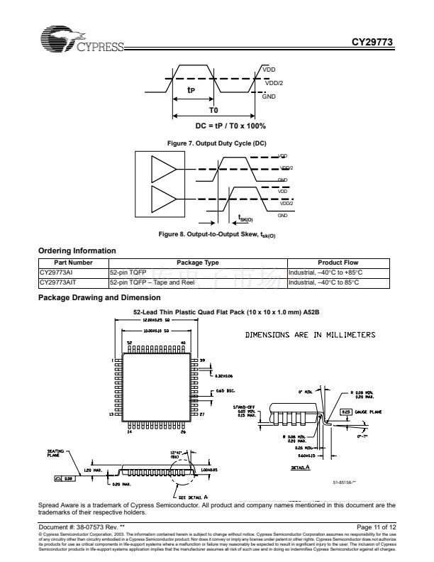
52-pin 1.0-mm TQFP package
Description
The CY29773 is a low-voltage high-performance 200-MHz
PLL-based zero delay buffer designed for high speed clock
distribution applications.
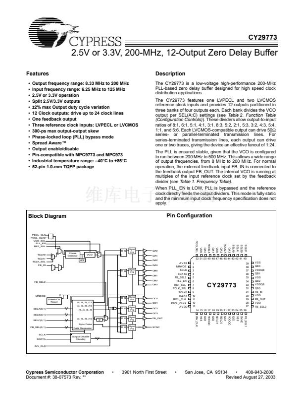
The CY29773 features one LVPECL and two LVCMOS
reference clock inputs and provides 12 outputs partitioned in
three banks of four outputs each. Each bank divides the VCO
output per SEL(A:C) settings (see
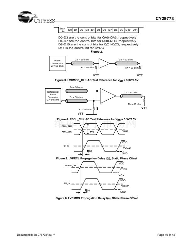
Table 2. Function Table
(Configuration Controls)).
These dividers allow output-to-input
ratios of 8:1, 6:1, 5:1, 4:1, 3:1, 8:3, 5:2, 2:1, 5:3, 3:2, 4:3, 5:4,
1:1, and 5:6. Each LVCMOS-compatible output can drive 50鈩?/div>
series- or parallel-terminated transmission lines. For
series-terminated transmission lines, each output can drive
one or two traces, giving the device an effective fanout of 1:24.
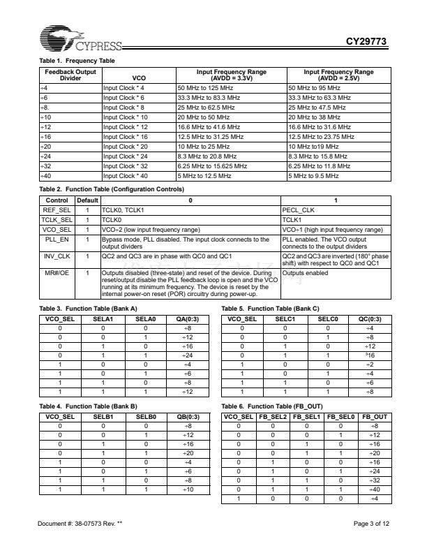
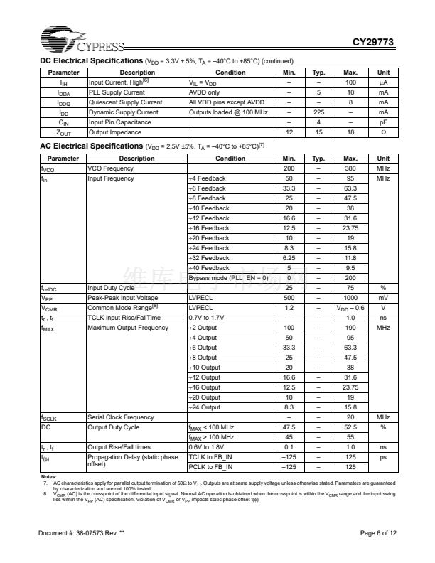
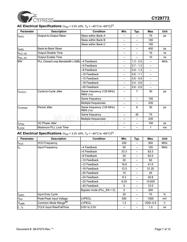
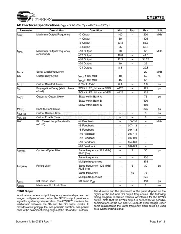
The PLL is ensured stable, given that the VCO is configured
to run between 200 MHz to 500 MHz. This allows a wide range
of output frequencies, from 8 MHz to 200 MHz. For normal
operation, the external feedback input FB_IN is connected to
the feedback output FB_OUT. The internal VCO is running at
multiples of the input reference clock set by the feedback
divider (see
Table 1. Frequency Table).
When PLL_EN is LOW, PLL is bypassed and the reference
clock directly feeds the output dividers. This mode is fully static
and the minimum input clock frequency specification does not
apply.
Block Diagram
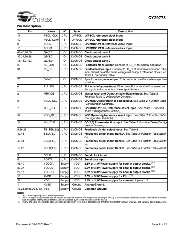
Pin Configuration
PECL_CLK
PECL_CLK#
VCO_SEL
PLL_EN
REF_SEL
D Q
TCLK0
TCLK1
TCLK_SEL
FB_IN
D Q
Sync
Frz
0
1
Phase
Detector
LPF
VCO
0
1
Sync
Frz
QA0
QA1
QA2
QA3
QB0
QB1
FB_SEL2
QB2
QB3
VCO_SEL
VDDQA
VDDQA
SELA0
SELA1
SELB0
SELB1
52 51 50 49 48 47 46 45 44 43 42 41 40
A V SS
MR#/OE
SCLK
SDA TA
FB_SEL2
PLL_EN
REF_SEL
TCLK_SEL
TCLK0
TCLK1
PECL_CLK
PECL_CLK#
A V DD
1
2
3
4
5
6
7
8
9
10
11
12
13
39
38
37
36
35
34
33
32
31
30
29
28
27
V SS
QB0
V DDQB
QB1
V SS
QB2
V DDQB
QB3
FB_IN
V SS
FB_OUT
V DD
FB_SEL0
VSS
QA0
C Y29773
QA1
VSS
QA2
QA3
MR#/OE
Power-On
Reset
SELA(0,1)
SELB(0,1)
SELC(0,1)
FB_SEL(0,1)
SCLK
SDATA
INV_CLK
Output Disable
Circuitry
12
2
2
2
2
/4, /6, /8, /10
Sync Pulse
Data Generator
D Q
/2
0
1
D Q
D Q
/4, /6, /8, /12
/4, /6, /8, /10
/2, /4, /6, /8
D Q
Sync
Frz
QC0
QC1
Sync
Frz
Sync
Frz
Sync
Frz
QC2
QC3
14 15 16 17 18 19 20 21 22 23 24 25 26
INV_CLK
VSS
QC3
VDDQC
QC2
SELC1
SELC0
QC1
VDDQC
QC0
VSS
SYNC
FB_SEL1
FB_OUT
SYNC
Cypress Semiconductor Corporation
Document #: 38-07573 Rev. **
鈥?/div>
3901 North First Street
鈥?/div>
San Jose
,
CA 95134
鈥?/div>
408-943-2600
Revised August 27, 2003


 1
1
 2
2
 3
3
 4
4
 5
5
 6
6
 7
7
 8
8
 9
9
 10
10
 11
11
 12
12
