鈥?/div>
Integrated phase-locked loop (PLL)
Low-jitter, high-accuracy outputs
VCXO with Analog Adjust
3.3V operation
Benefits
鈥?Internal PLL with up to 400-MHz internal operation
鈥?Meets critical timing requirements in complex system
designs
鈥?Large 鹵200-ppm range, better linearity
鈥?Enables application compatibility
Output Frequency Range
Two copies of 27-MHz reference clock output, two copies of
54/53.946053/67.425/67.357642 MHz (frequency selectable)
Two copies of 27-MHz reference clock output, two copies of
54/53.946053/67.425/68.400599 MHz (frequency selectable)
Part Number
CY24207-1
CY24207-2
Outputs
4
4
Input Frequency
27-MHz Crystal Input
27-MHz Crystal Input
Block Diagram
XIN
XOUT
VCXO
P
桅
VCO
OUTPUT
MULTIPLEXER
AND
DIVIDERS
CLK1
CLK2
REFCLK1
REFCLK2
Pin Configuration
16-pin TSSOP
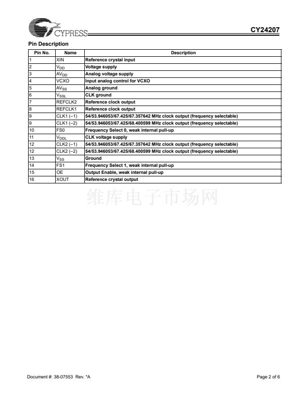
XIN
VDD
AVDD
VCXO
AVSS
VSSL
REFCLK2
REFCLK1
1
2
16
15
XOUT
OE
FS1
VSS
CLK1
VDDL
FS0
CLK2
OSC.
Q
24207-1,-2
3
4
5
6
7
8
14
13
12
11
10
9
PLL
FS0
FS1
OE
VDDL
VDD
AVDD
AVSS
VSS
VSSL
Frequency Select Options
OE
0
0
0
0
1
1
1
1
FS1
0
0
1
1
0
0
1
1
FS0
0
1
0
1
0
1
0
1
CLK1/CLK2 (-1)
[1]
off
off
off
off
54
53.946053 (鈥? ppm)
67.425
67.357642 (3.8 ppm)
CLK1/CLK2 (-2)
[1]
off
off
off
off
54
53.946053 (鈥? ppm)
67.425
68.400599(鈥?.8 ppm)
REFCLK 1/2
27
27
27
27
27
27
27
27
Unit
MHz
MHz
MHz
MHz
MHz
MHz
MHz
MHz
Note:
1. 鈥渙ff鈥?= output is driven high.
Cypress Semiconductor Corporation
Document #: 38-07553 Rev. *A
鈥?/div>
3901 North First Street
鈥?/div>
San Jose
,
CA 95134
鈥?/div>
408-943-2600
Revised July 31, 2003


 1
1
 2
2
 3
3
 4
4
 5
5
 6
6
