鈥?/div>
Low power consumption 80mW
(200鈩?load at 2Vp-p output)
Structure
Silicon gate CMOS IC
Function
6-bit 40MHz D/A converter
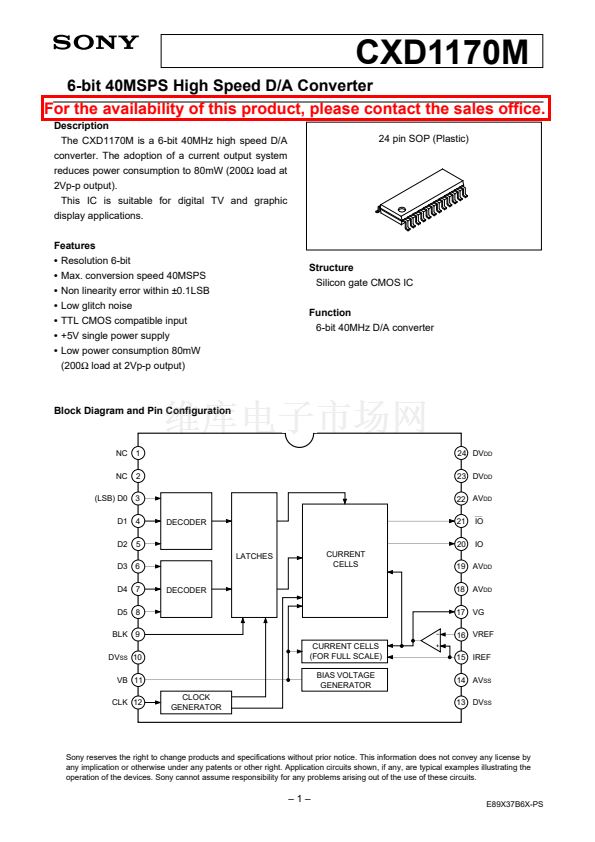
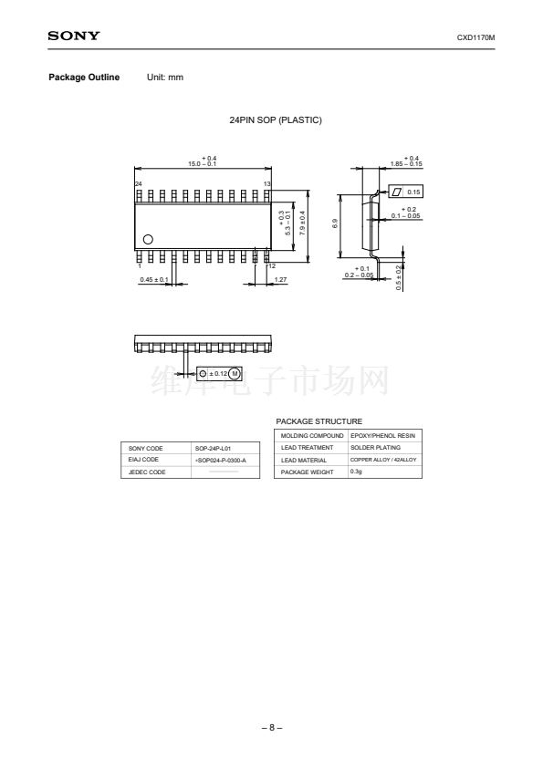
24 pin SOP (Plastic)
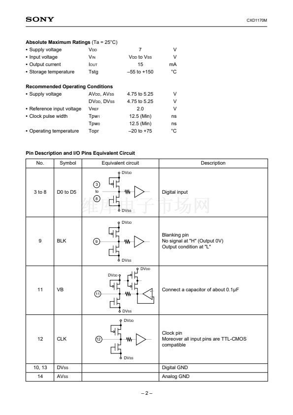
Block Diagram and Pin Configuration
NC
NC
1
2
24 DV
DD
23 DV
DD
22 AV
DD
DECODER
21
20
LATCHES
CURRENT
CELLS
IO
IO
(LSB) D0 3
D1
D2
4
5
D3 6
D4
D5
7
8
DECODER
19 AV
DD
18 AV
DD
17 VG
16 VREF
BLK 9
DV
SS
10
VB 11
CLK 12
CLOCK
GENERATOR
CURRENT CELLS
(FOR FULL SCALE)
BIAS VOLTAGE
GENERATOR
15 IREF
14 AV
SS
13 DV
SS
Sony reserves the right to change products and specifications without prior notice. This information does not convey any license by
any implication or otherwise under any patents or other right. Application circuits shown, if any, are typical examples illustrating the
operation of the devices. Sony cannot assume responsibility for any problems arising out of the use of these circuits.
next


 1
1
 2
2
 3
3
 4
4
 5
5
 6
6
 7
7
 8
8
