Semiconductor
January 1999
T
NT
DUC
PRO LACEME 747
7
ETE
P
SOL DED RE 800-442-
B
O
EN
om
s 1-
OMM lication harris.c
C
E
NO R ntral App entapp@
Ce
: c
Call or email
CA3256
25MHz, BiMOS Analog
Video Switch and Ampli鏗乪r
[ /Title
(CA32
56)
/Sub-
ject
(25MH
z,
BiMO
S Ana-
log
Video
Switch
and
Ampli-
鏗乪r)
/Autho
r ()
/Key-
words
(Har-
ris
Semi-
con-
ductor,
4x1,
video
cross-
point
switch,
multi-
plexer
multi-
plexor,
cable
driver,
5x1,
moni
tor out-
put,
adjust-
able
gain,
Features
鈥?5 Multiplex Video Channels
- 1 Independent Channel
- 4 Channels with Enable
鈥?4 LED Channel Indicator Outputs
鈥?Wideband Video Ampli鏗乪r . . . . . . . . 25MHz Unity Gain
鈥?Adjustable Video Ampli鏗乪r Gain
鈥?High Signal-Drive Capability
Description
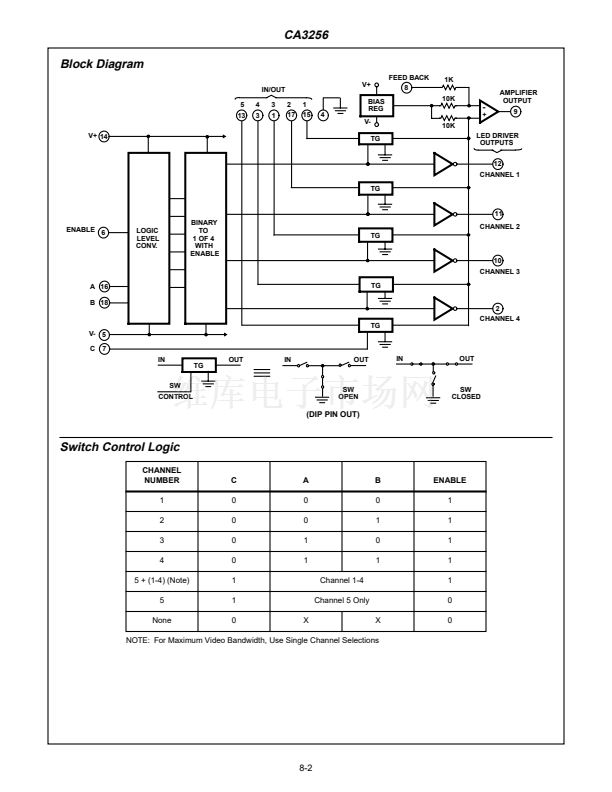
The CA3256 BiMOS analog video switch has 鏗乿e channels
of CMOS multiplex switching for general-purpose video-
signal control. One of four CMOS channels may be selected
in parallel with channel 5. The CMOS switches are inputs to
the video ampli鏗乪r but may be used in bilateral switching
between channels 1 to 4 and channel 5. The analog
switches of channels 1 to 4 are digitally controlled with logic
level conversion and binary decoding to select 1 of 4
channels. The enable function controls channels 1 to 4 but
does not affect channel 5. LED output drivers are selected
with the channel 1-to-4 switch selection to indicate the ON-
channel. Channel 5 may be used as a monitor output for
data or signal information on channels 1 to 4. The
transmission gate switches shown in the block diagram of
the CA3256 are con鏗乬ured in a 鈥淭鈥?design to minimize
feedthrough. When the switch is off, the shunt or center of
the 鈥淭鈥?is grounded.
The ampli鏗乪r has high input impedance to minimize the R
ON
transmission gate insertion loss. The ampli鏗乪r output imped-
ance is typically 5鈩?in a complementary symmetry output.
The ampli鏗乪r can directly drive a nominal 75鈩?coaxial cable
to provide line-to-line video switching. The gain of the ampli-
鏗乪r is programmable by different feedback resistor values
between pins 8 and 9. Compensation may also be used
between these pins for an optimally 鏗俛t frequency response.
An internal regulated 5V bias reference with temperature
compensation permits stable direct-coupled output drive and
minimizes DC offset during signal switching.
Applications
鈥?Video Multiplex Switch
鈥?75鈩?Video Ampli鏗乪r/Line Driver
鈥?Video Signal-Level Control
鈥?Monitor Switching Control
鈥?TV/CATV Audio/Video Switch
鈥?Video Signal Adder/Fader Control
Part Number Information
PART NUMBER
CA3256E
CA3256M
TEMP.
RANGE (
o
C)
-40 to 85
-40 to 85
PACKAGE
18 Ld PDIP
20 Ld SOIC
PKG.
NO.
E18.3
M20.3
Pinouts
CA3256
(PDIP)
TOP VIEW
CA3256
(SOIC)
TOP VIEW
IN 3
LED 4
IN 4
GND
V-
ENABLE
CONTROL C
FEEDBACK
AMP OUT
1
2
3
4
5
6
7
8
9
18 CONTROL B
17 IN 2
16 CONTROL A
15 IN 1
14 V+
13 IN/OUT 5
12 LED 1
11 LED 2
10 LED 3
IN3
LED4
IN4
GND
V-
ENABLE
CONTROL C
FEEDBACK
AMP OUT
1
2
3
4
5
6
7
8
9
20 CONTROL B
19 IN2
18 CONTROL A
17 NC
16 IN1
15 V+
14 IN/OUT5
13 NC
12 LED1
11 LED2
LED3 10
CAUTION: These devices are sensitive to electrostatic discharge. Users should follow proper IC Handling Procedures.
Copyright
漏
Harris Corporation 1999
File Number
1769.5
8-1


 1
1
 2
2
 3
3
 4
4
 5
5
 6
6
 7
7
 8
8
 9
9
 10
10
 11
11
