Philips Semiconductors
Product specification
PowerMOS transistor
Logic level FET
GENERAL DESCRIPTION
N-channel enhancement mode logic
level field-effect power transistor in a
plastic envelope suitable for surface
mount applications.
The device is intended for use in
Switched Mode Power Supplies
(SMPS), motor control, welding,
DC/DC and AC/DC converters, and in
automotive and general purpose
switching applications.
BUK565-60A
QUICK REFERENCE DATA
SYMBOL
V
DS
I
D
P
tot
T
j
R
DS(ON)
PARAMETER
Drain-source voltage
Drain current (DC)
Total power dissipation
Junction temperature
Drain-source on-state
resistance;
V
GS
= 5 V
MAX.
60
39
125
175
0.042
UNIT
V
A
W
藲C
鈩?/div>
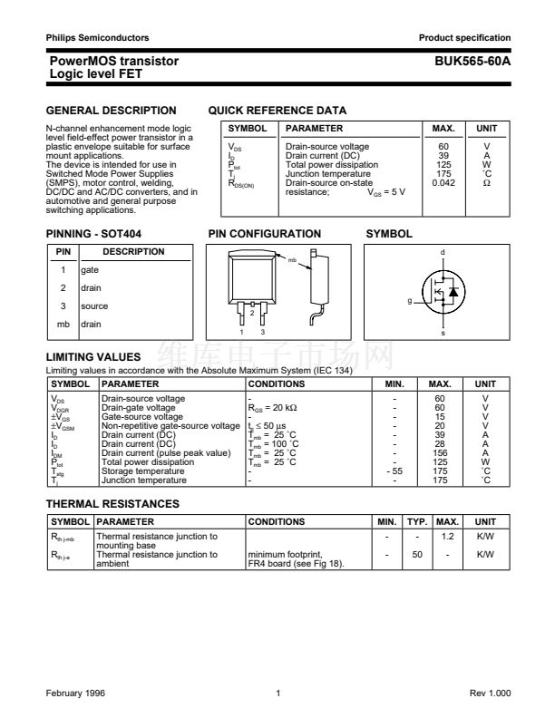
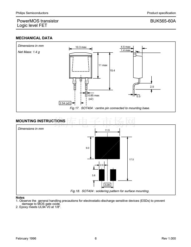
PINNING - SOT404
PIN
1
2
3
mb
gate
drain
source
drain
DESCRIPTION
PIN CONFIGURATION
mb
SYMBOL
d
g
2
1
3
s
LIMITING VALUES
Limiting values in accordance with the Absolute Maximum System (IEC 134)
SYMBOL
V
DS
V
DGR
鹵V
GS
鹵V
GSM
I
D
I
D
I
DM
P
tot
T
stg
T
j
PARAMETER
Drain-source voltage
Drain-gate voltage
Gate-source voltage
Non-repetitive gate-source voltage
Drain current (DC)
Drain current (DC)
Drain current (pulse peak value)
Total power dissipation
Storage temperature
Junction temperature
CONDITIONS
-
R
GS
= 20 k鈩?/div>
-
t
p
鈮?/div>
50
碌s
T
mb
= 25 藲C
T
mb
= 100 藲C
T
mb
= 25 藲C
T
mb
= 25 藲C
-
-
MIN.
-
-
-
-
-
-
-
-
- 55
-
MAX.
60
60
15
20
39
28
156
125
175
175
UNIT
V
V
V
V
A
A
A
W
藲C
藲C
THERMAL RESISTANCES
SYMBOL PARAMETER
R
th j-mb
R
th j-a
Thermal resistance junction to
mounting base
Thermal resistance junction to
ambient
CONDITIONS
MIN.
-
minimum footprint,
FR4 board (see Fig 18).
-
TYP. MAX.
-
50
1.2
-
UNIT
K/W
K/W
February 1996
1
Rev 1.000


 1
1
 2
2
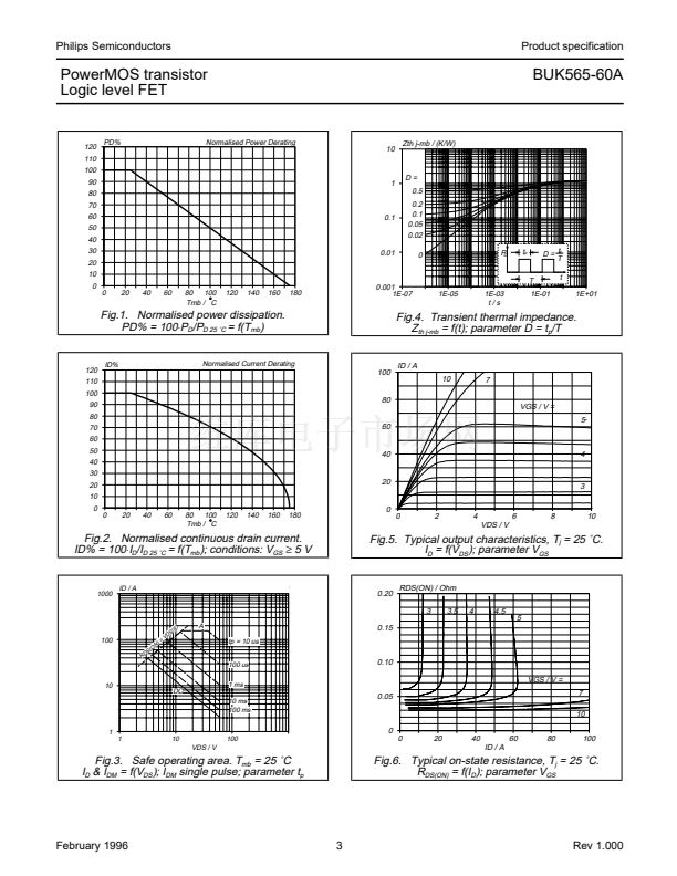 3
3
 4
4
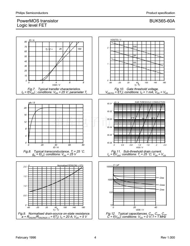
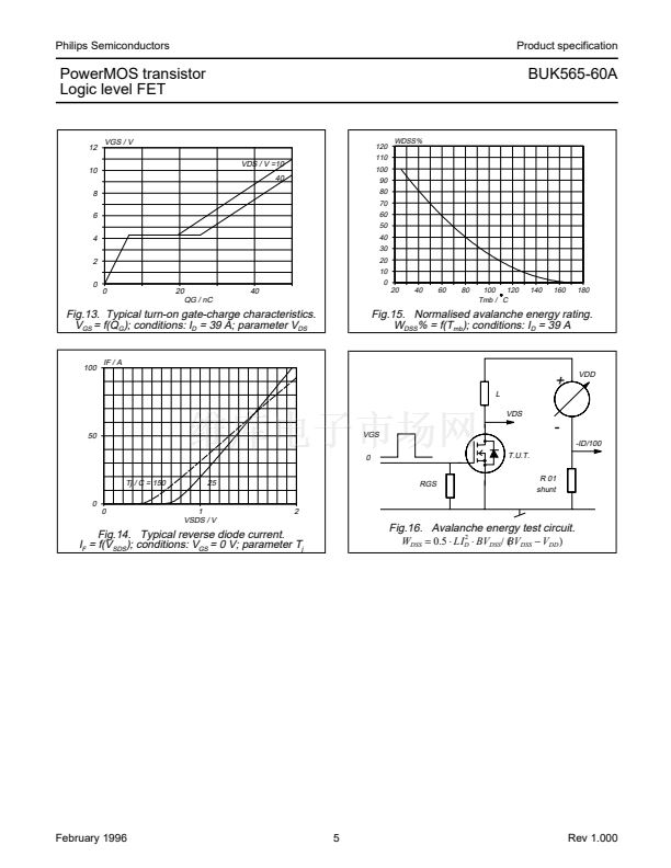 5
5
 6
6
 7
7
