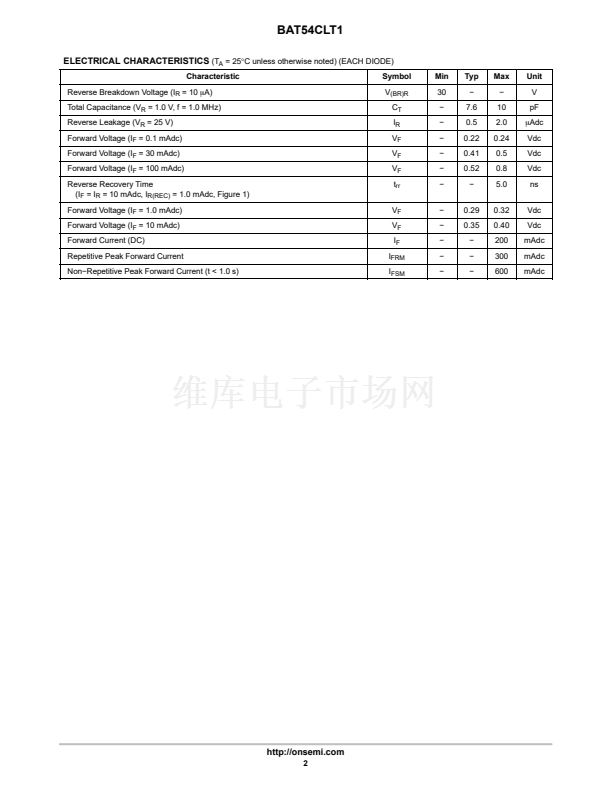
鈥?/div>
Low Forward Voltage 鈭?0.35 Volts (Typ) @ I
F
= 10 mAdc
30 VOLT
DUAL COMMON CATHODE
SCHOTTKY BARRIER DIODES
1
ANODE
3
CATHODE
2
ANODE
MAXIMUM RATINGS
(T
J
= 125擄C unless otherwise noted)
Rating
Reverse Voltage
Forward Power Dissipation
@ T
A
= 25擄C
Derate above 25擄C
Thermal Resistance,
Junction-to-Ambient
Forward Current (DC)
Junction Temperature
Storage Temperature Range
Symbol
V
R
P
F
225
1.8
R
qJA
I
F
T
J
T
stg
508 (Note 1)
311 (Note 2)
200 Max
125 Max
鈭?5 to +150
mW
mW/擄C
擄C/W
mA
擄C
擄C
5C
M
= Device Code
= Date Code
1
2
Value
30
Unit
V
3
SOT鈭?3
CASE 318
STYLE 9
1
MARKING
DIAGRAM
3
5C M
2
Maximum ratings are those values beyond which device damage can occur.
Maximum ratings applied to the device are individual stress limit values (not
normal operating conditions) and are not valid simultaneously. If these limits
are exceeded, device functional operation is not implied, damage may occur
and reliability may be affected.
1. FR鈭? @ Minimum Pad.
2. FR鈭? @ 1.0 x 1.0 inch Pad.
ORDERING INFORMATION
Device
BAT54CLT1
BAT54CLT1G
Package
SOT鈭?3
SOT鈭?3
(Pb鈭扚ree)
Shipping
鈥?/div>
3000/Tape & Reel
3000/Tape & Reel
鈥燜or information on tape and reel specifications,
including part orientation and tape sizes, please
refer to our Tape and Reel Packaging Specifications
Brochure, BRD8011/D.
Preferred
devices are recommended choices for future use
and best overall value.
漏
Semiconductor Components Industries, LLC, 2004
1
September, 2004 鈭?Rev. 2
Publication Order Number:
BAT54SLT1/D


 1
1
 2
2
 3
3
 4
4
