鈥?/div>
Industry Standard Architecture
Low Cost Easy-to-Use Software Tools
High Speed Electrically Erasable Programmable Logic Devices
5 ns Maximum Pin-to-Pin Delay
CMOS and TTL Compatible Inputs and Outputs
Latch Feature Holds Inputs to Previous Logic States
Advanced Flash Technology
Reprogrammable
100% Tested
High Reliability CMOS Process
20 Year Data Retention
100 Erase/Write Cycles
2,000V ESD Protection
200 mA Latchup Immunity
Dual-in-Line and Surface Mount Packages in Standard Pinouts
High
Performance
E
2
PLD
ATF22V10C
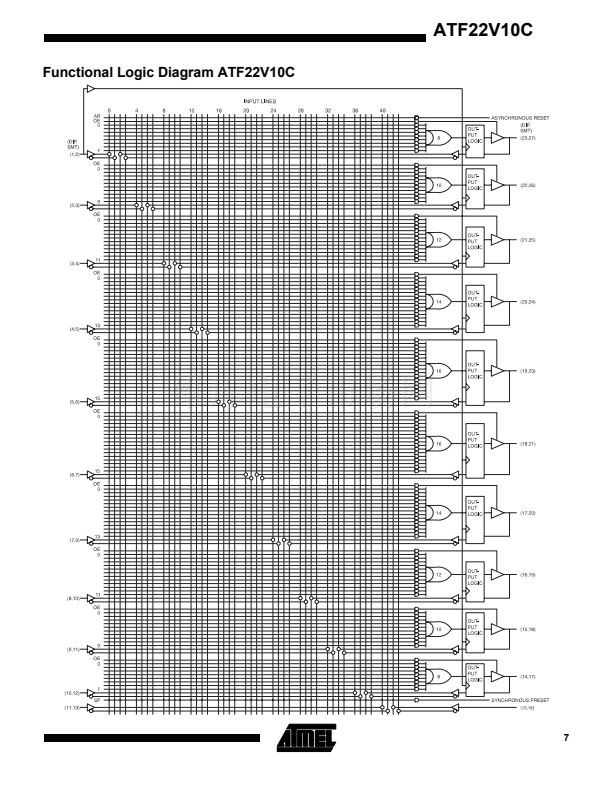
Logic Diagram
Pin Configurations
Pin Name
CLK
IN
I/O
*
VCC
PD
Function
Clock
Logic Inputs
Bidirectional Buffers
No Internal Connection
+5V Supply
Power Down
CLK/IN
IN
IN
IN/PD
IN
IN
IN
IN
IN
IN
IN
GND
1
2
3
4
5
6
7
8
9
10
11
12
24
23
22
21
20
19
18
17
16
15
14
13
VCC
I/O
I/O
I/O
I/O
I/O
I/O
I/O
I/O
I/O
I/O
IN
TSSOP Top View
ATF22V10C
DIP/SOIC
PLCC
Top view
Note:
For PLCC, pins 1, 8, 15 and 22 can be left uncon-
nected. For superior performance, connect V
CC
to pin 1 and ground to 8, 15, 22.
Rev. 0735C/22V10C-D鈥?4/98


 1
1
 2
2
 3
3
 4
4
 5
5
 6
6
 7
7
 8
8
