鈥?/div>
鈥?Available in 8M Bits (AT49LL080), 4M Bits (AT49LL040) and 2M Bits (AT49LL020)
鈥?Automated Byte-program and Sector-erase Operations
Two Configurable Interfaces
鈥?Low Pin Count (LPC) Interface for In-System Operation
鈥?Address/Address Multiplexed (A/A Mux) Interface for Programming during
Manufacturing
Low Pin Count Hardware Interface Mode
鈥?5-signal Communication Interface Supporting x8 Reads and Writes
鈥?Read and Write Protection for Each Sector Using Software-controlled Registers
鈥?Two Hardware Write-protect Pins: One for the Top Boot Sector, One for All Other
Sectors
鈥?Five General-purpose Inputs, GPIs, for Platform Design Flexibility
鈥?Operates with 33 MHz PCI Clock and 3.3V I/O
Address/Address Multiplexed (A/A Mux) Interface
鈥?11-pin Multiplexed Address and 8-pin Data Interface
鈥?Supports Fast On-board or Out-of-system Programming
Power Supply Specifications
鈥?V
CC
: 3.3V 鹵 0.3V
鈥?V
PP
: 3.3V and 12V for Fast Programming
Industry-standard Package
鈥?40-lead TSOP or 32-lead PLCC
鈥?/div>
鈥?/div>
鈥?/div>
鈥?/div>
8-megabit,
4-megabit and
2-megabit
Low-pin Count
Flash Memory
AT49LL080
AT49LL040
AT49LL020
Description
The AT49LL080, AT49LL040 and the AT49LL020 are Flash memory devices designed
to interface with the LPC bus for PC Applications. A feature of the AT49LL080/040/020
is the nonvolatile memory core. The high-performance memory is arranged in sixteen
(AT49LL080), eleven (AT49LL040) sectors or seven (AT49LL020) (see page 11).
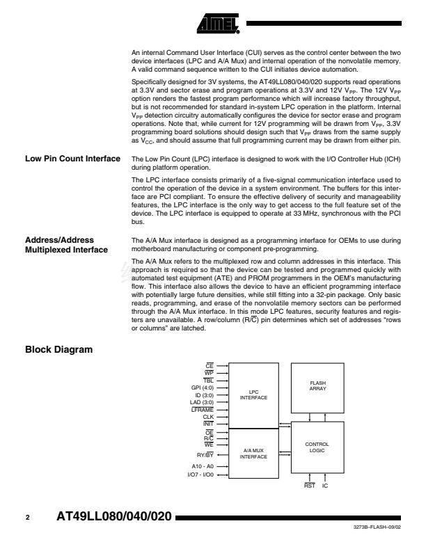
The AT49LL080/040/020 supports two hardware interfaces: Low Pin Count (LPC) for
in-system operation and Address/Address Multiplexed (A/A Mux) for programming
during manufacturing. The IC (Interface Configuration) pin of the device provides the
control between the interfaces. The interface mode needs to be selected prior to
power-up or before return from reset (RST or INIT low to high transition).
Pin Configuration
PLCC
GPI2 [A8]
GPI3 [A9]
RST [RST]
VPP [VPP]
VCC [VCC]
CLK [R/C]
GPI4 [A10]
(NC) CE
[IC (V
IH
)] IC (V
IL
)
[NC] NC
[NC] NC
[NC] NC
[NC] NC
[A10] GPI4
[NC] NC
[R/C] CLK
[VCC] VCC
[VPP] VPP
[RST] RST
[NC] NC
[NC] NC
[A9] GPI3
[A8] GPI2
[A7] GPI1
[A6] GPI0
[A5] WP
[A4] TBL
1
2
3
4
5
6
7
8
9
10
11
12
13
14
15
16
17
18
19
20
TSOP, Type I
40
39
38
37
36
35
34
33
32
31
30
29
28
27
26
25
24
23
22
21
GNDa [GNDa]
VCCa [VCCa]
LFRAME [WE]
INIT [OE]
RFU [RY/BY]
RFU [I/O7]
RFU [I/O6]
RFU [I/O5]
RFU [I/O4]
VCC [VCC]
GND [GND]
GND [GND]
LAD3 [I/O3]
LAD2 [I/O2]
LAD1 [I/O1]
LAD0 [I/O0]
ID0* [A0]
ID1* [A1]
ID2* [A2]
ID3* [A3]
[I/O1] LAD1
[I/O2] LAD2
[GND] GND
[I/O3] LAD3
[I/O4] RFU
[I/O5] RFU
[I/O6] RFU
14
15
16
17
18
19
20
[A7] GPI1
[A6] GPI0
[A5] WP
[A4] TBL
[A3] ID3*
[A2] ID2*
[A1] ID1*
[A0] ID0*
[I/O0] LAD0
5
6
7
8
9
10
11
12
13
4
3
2
1
32
31
30
29
28
27
26
25
24
23
22
21
IC (V
IL
) [IC(V
IH
)]
CE [NC]
NC
NC
VCC [VCC]
INIT [OE]
LFRAME [WE]
RFU [RY/BY]
RFU [I/O7]
[ ] Designates A/A Mux Mode
[ ] Designates A/A Mux Mode
Rev. 3273B鈥揊LASH鈥?9/02
Note:
*The ID Pins are Not Available on the AT49LL020.
ID0 is Not Available on the AT49LL080.
1


 1
1
 2
2
 3
3
 4
4
 5
5
 6
6
 7
7
 8
8
 9
9
 10
10
 11
11
 12
12
 13
13
 14
14
 15
15
 16
16
 17
17
 18
18
 19
19
 20
20
 21
21
 22
22
 23
23
 24
24
 25
25
 26
26
 27
27
 28
28
 29
29
 30
30
 31
31
 32
32
