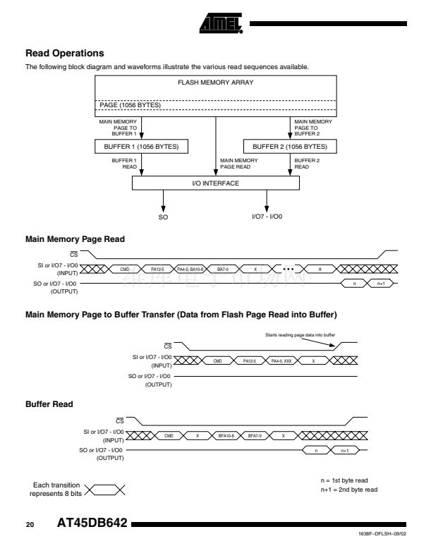
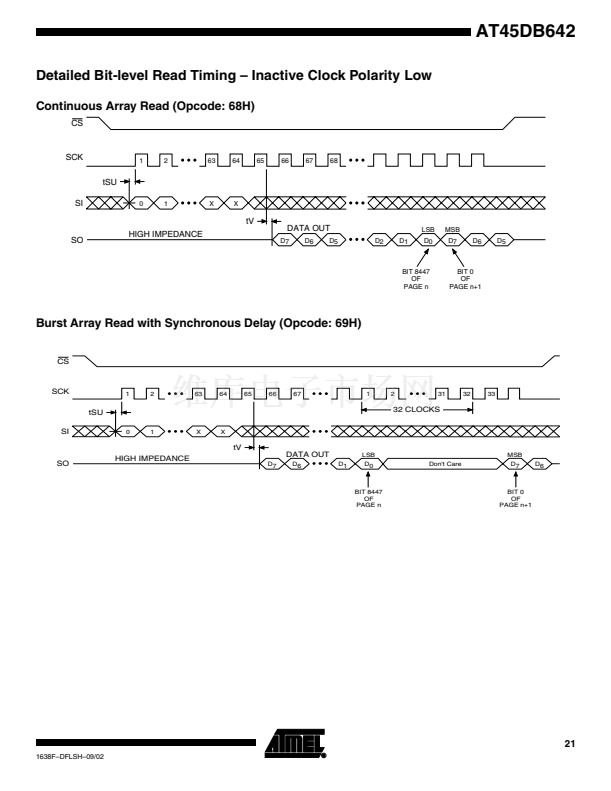
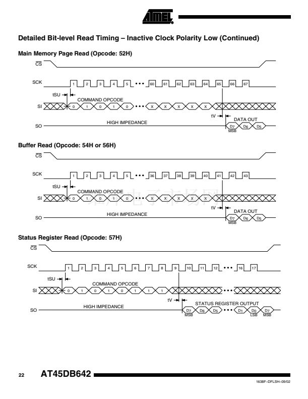
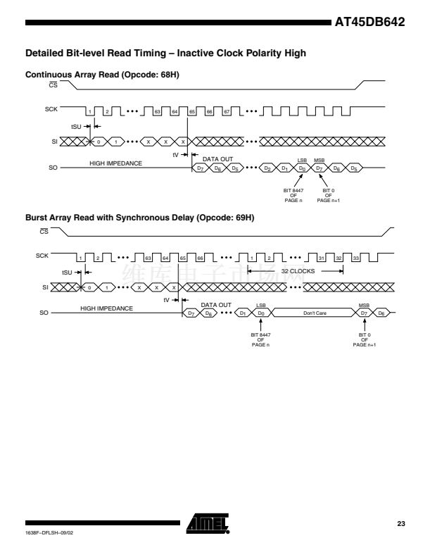
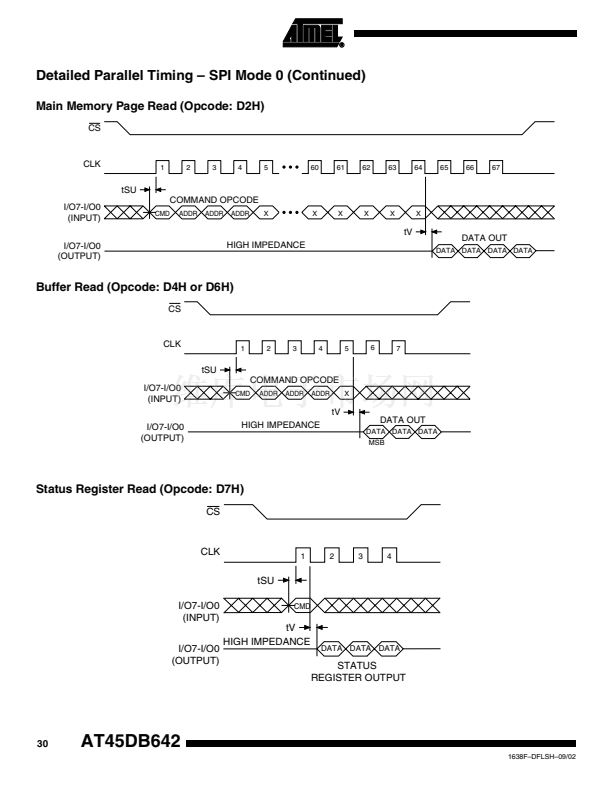
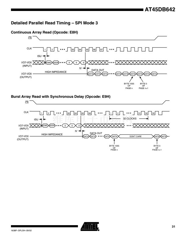
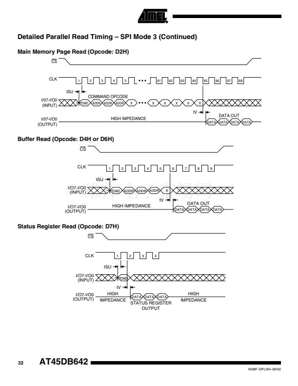
鈥?/div>
鈥?Dedicated Serial Interface (SPI Modes 0 and 3 Compatible)
鈥?Dedicated Parallel I/O Interface (Optional Use)
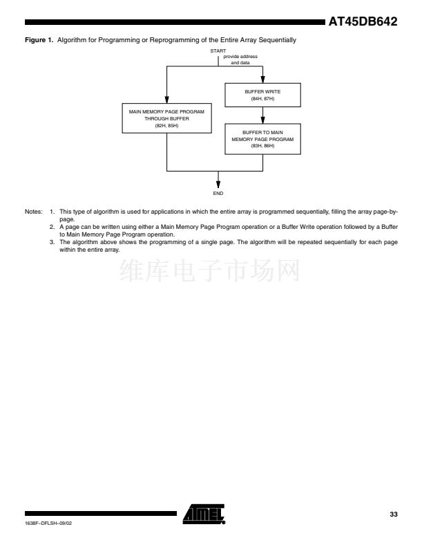
Page Program Operation
鈥?Single Cycle Reprogram (Erase and Program)
鈥?8192 Pages (1056 Bytes/Page) Main Memory
Supports Page and Block Erase Operations
Two 1056-byte SRAM Data Buffers 鈥?Allows Receiving of Data
while Reprogramming the Flash Array
Continuous Read Capability through Entire Array
鈥?Ideal for Code Shadowing Applications
Low-power Dissipation
鈥?4 mA Active Read Current Typical
鈥?2 碌A(chǔ) CMOS Standby Current Typical
20 MHz Maximum Clock Frequency 鈥?Serial Interface
5 MHz Maximum Clock Frequency 鈥?Parallel Interface
Hardware Data Protection
Commercial and Industrial Temperature Ranges
64-megabit
2.7-volt Only
Dual-interface
DataFlash
廬
AT45DB642
Description
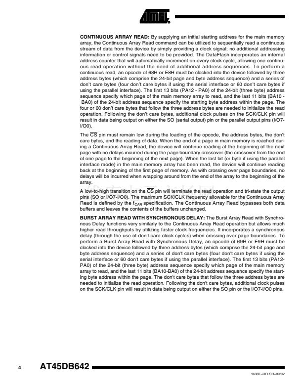
The AT45DB642 is a 2.7-volt only, dual-interface Flash memory ideally suited for a
wide variety of digital voice-, image-, program code- and data-storage applications. The
dual-interface of the AT45DB642 allows a dedicated serial interface to be connected to a
DSP and a dedicated parallel interface to be connected to a microcontroller or vice versa.
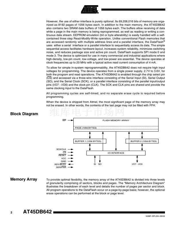
Pin Configurations
Pin Name
CS
SCK/CLK
SI
SO
I/O7 - I/O0
WP
RESET
RDY/BUSY
SER/PAR
Function
Chip Select
Serial Clock/Clock
Serial Input
Serial Output
Parallel Input/Output
Hardware Page Write Protect Pin
Chip Reset
Ready/Busy
Serial/Parallel Interface Control
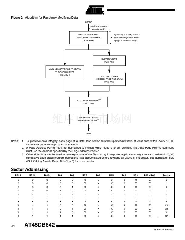
Note:
NC
NC
RDY/BUSY
RESET
WP
NC
NC
NC
VCC
GND
NC
NC
NC
NC
CS
SCK/CLK
SI*
SO*
NC
NC
1
2
3
4
5
6
7
8
9
10
11
12
13
14
15
16
17
18
19
20
TSOP Top View
Type 1
40
39
38
37
36
35
34
33
32
31
30
29
28
27
26
25
24
23
22
21
NC
NC
NC
NC
NC
I/O7*
I/O6*
I/O5*
I/O4*
VCCP*
GNDP*
I/O3*
I/O2*
I/O1*
I/O0*
SER/PAR*
NC
NC
NC
NC
DataFlash Card
7 6 5 4 3 2 1
(1)
*Optional Use 鈥?See pin description
text for connection information.
Note:
1. See AT45DCB008 Datasheet.
Rev. 1638F鈥揇FLSH鈥?9/02
1


 1
1
 2
2
 3
3
 4
4
 5
5
 6
6
 7
7
 8
8
 9
9
 10
10
 11
11
 12
12
 13
13
 14
14
 15
15
 16
16
 17
17
 18
18
 19
19
 20
20
 21
21
 22
22
 23
23
 24
24
 25
25
 26
26
 27
27
 28
28
 29
29
 30
30
 31
31
 32
32
 33
33
 34
34
 35
35
 36
36
 37
37
