鈥?/div>
鈥?Single Cycle Reprogram (Erase and Program)
鈥?4096 Pages (528 Bytes/Page) Main Memory
Optional Page and Block Erase Operations
Two 528-Byte SRAM Data Buffers 鈥?Allows Receiving of Data
while Reprogramming of Nonvolatile Memory
Internal Program and Control Timer
Fast Page Program Time 鈥?7 ms Typical
120
碌
s Typical Page to Buffer Transfer Time
Low Power Dissipation
鈥?4 mA Active Read Current Typical
鈥?3
碌
A CMOS Standby Current Typical
13 MHz Max Clock Frequency
Hardware Data Protection Feature
Serial Peripheral Interface (SPI) Compatible 鈥?Modes 0 and 3
CMOS and TTL Compatible Inputs and Outputs
Commercial and Industrial Temperature Ranges
16-Megabit
2.7-volt Only
Serial
DataFlash
廬
AT45DB161
Preliminary
Description
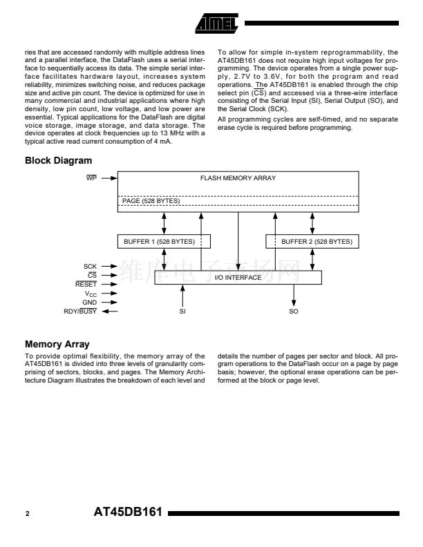
The AT45DB161 is a 2.7-volt only, serial interface Flash memory suitable for in-sys-
tem reprogramming. Its 17,301,504 bits of memory are organized as 4096 pages of
528 bytes each. In addition to the main memory, the AT45DB161 also contains two
SRAM data buffers of 528 bytes each. The buffers allow receiving of data while a
page in the main memory is being reprogrammed. Unlike conventional Flash memo-
(continued)
Pin Configurations
Pin Name
CS
SCK
SI
SO
WP
RESET
RDY/BUSY
Function
Chip Select
Serial Clock
Serial Input
Serial Output
Hardware Page
Write Protect Pin
Chip Reset
Ready/Busy
GND
NC
NC
CS
SCK
SI
SO
NC
NC
NC
NC
NC
NC
NC
SOIC
1
2
3
4
5
6
7
8
9
10
11
12
13
14
28
27
26
25
24
23
22
21
20
19
18
17
16
15
VCC
NC
NC
WP
RESET
RDY/BUSY
NC
NC
NC
NC
NC
NC
NC
NC
CBGA Top View
Through Package
1
2
3
4
5
A
NC
NC
NC
NC
NC
NC
B
NC
SCK GND VCC
CS RDY/BSY WP
SO
NC
C
NC
D
NC
SI RESET NC
NC
NC
NC
E
NC
PLCC
CS
NC
NC
GND
VCC
NC
NC
RDY/BUSY
RESET
WP
NC
NC
VCC
GND
NC
NC
NC
CS
SCK
SI
SO
1
2
3
4
5
6
7
8
9
10
11
12
13
14
TSOP Top View
Type 1
WP
RESET
RDY/BUSY
NC
NC
NC
NC
NC
NC
28
27
26
25
24
23
22
21
20
19
18
17
16
15
NC
NC
NC
NC
NC
NC
NC
NC
NC
NC
NC
NC
NC
NC
AT45DB161
Preliminary 16-
Megabit 2.7-volt
Only Serial
DataFlash
NC
NC
DC
DC
NC
NC
NC
14
15
16
17
18
19
20
SCK
SI
SO
NC
NC
NC
NC
NC
NC
5
6
7
8
9
10
11
12
13
4
3
2
1
32
31
30
29
28
27
26
25
24
23
22
21
Rev. 0807C鈥?7/98
Note: PLCC package pins 16
and 17 are DON鈥橳 CONNECT
1


 1
1
 2
2
 3
3
 4
4
 5
5
 6
6
 7
7
 8
8
 9
9
 10
10
 11
11
 12
12
 13
13
 14
14
 15
15
 16
16
 17
17
 18
18
 19
19
 20
20
