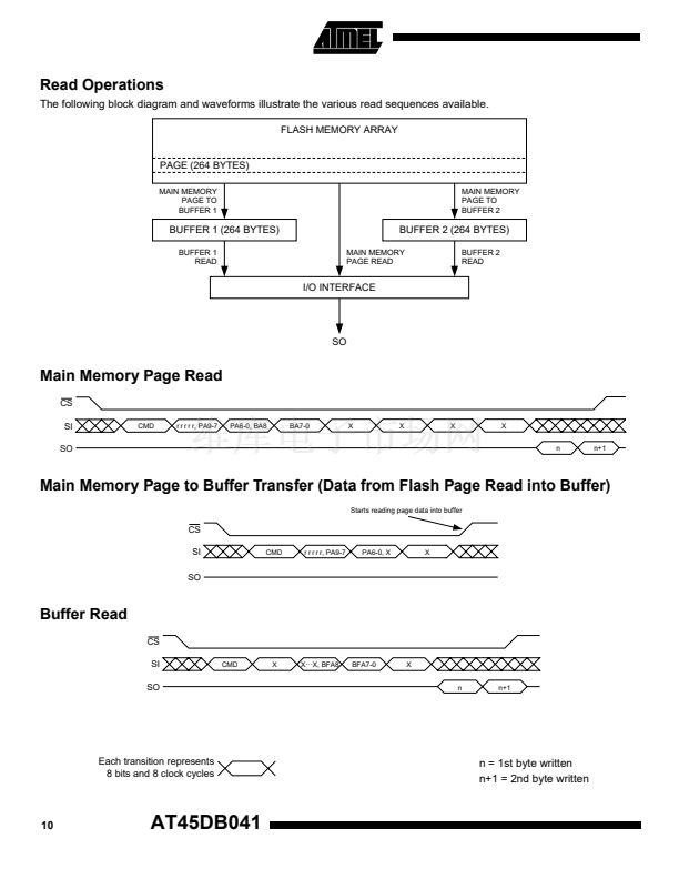
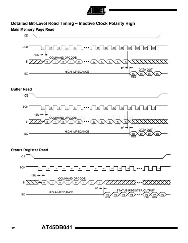
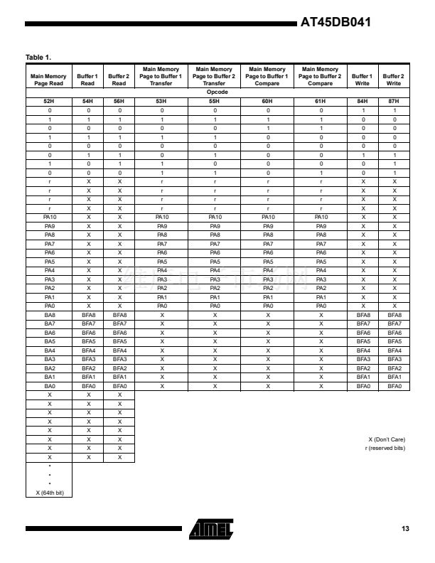
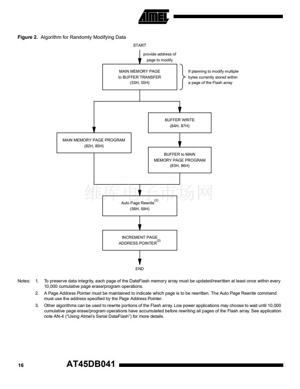
鈥?/div>
鈥?Single Cycle Reprogram (Erase and Program)
鈥?2048 Pages (264 Bytes/Page) Main Memory
Two 264-Byte SRAM Data Buffers 鈥?Allows Receiving of Data
While Reprogramming of Non-Volatile Memory
Internal Program and Control Timer
Fast Page Program Time 鈥?7 ms Typical
120
碌
s Typical Page to Buffer Transfer Time
Low Power Dissipation
鈥?4 mA Active Read Current Typical
鈥?8
碌
A CMOS Standby Current Typical
5 MHz Max Clock Frequency
Hardware Data Protection Feature
Serial Peripheral Interface (SPI) Compatible 鈥?Modes 0 and 3
CMOS and TTL Compatible Inputs and Outputs
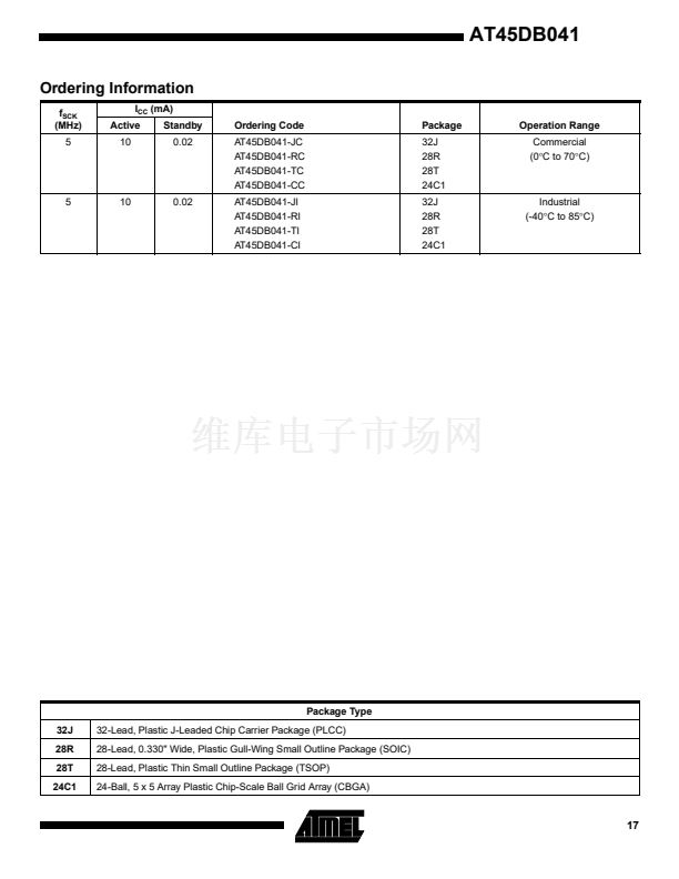
Commercial and Industrial Temperature Ranges
4-Megabit
2.7-volt Only
Serial
DataFlash
廬
AT45DB041
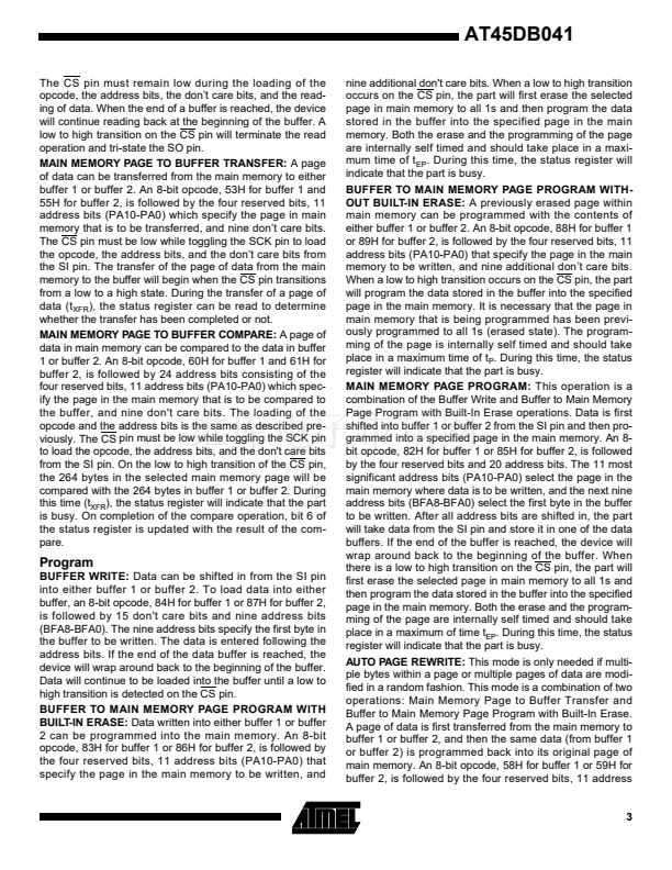
Description
The AT45DB041 is a 2.7-volt only, serial interface Flash memory suitable for in-sys-
tem reprogramming. Its 4,325,376 bits of memory are organized as 2048 pages of
264-bytes each. In addition to the main memory, the AT45DB041 also contains two
SRAM data buffers of 264-bytes each. The buffers allow receiving of data while a
page in the main memory is being reprogrammed. Unlike conventional Flash memo-
ries that are accessed randomly with multiple address lines and a parallel interface,
the DataFlash uses a serial interface to sequentially access its data. The simple serial
interface facilitates hardware layout, increases system reliability, minimizes switching
(continued)
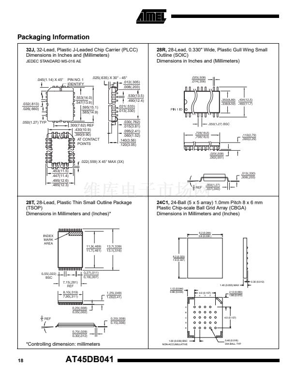
Pin Configurations
PLCC
SOIC
CS
NC
NC
GND
VCC
NC
NC
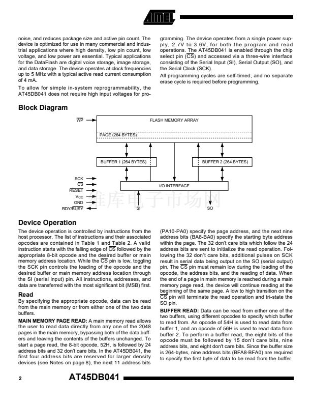
Pin Name
CS
SCK
SI
SO
WP
RESET
RDY/BUSY
Function
Chip Select
Serial Clock
Serial Input
Serial Output
Hardware Page Write
Protect Pin
Chip Reset
Ready/Busy
SCK
SI
SO
NC
NC
NC
NC
NC
NC
Note: PLCC package pins 16
and 17 are DON鈥橳 CONNECT.
TSOP Top View
Type 1
RDY/BUSY
RESET
WP
NC
NC
VCC
GND
NC
NC
NC
CS
SCK
SI
SO
1
2
3
4
5
6
7
8
9
10
11
12
13
14
28
27
26
25
24
23
22
21
20
19
18
17
16
15
NC
NC
NC
NC
NC
NC
NC
NC
NC
NC
NC
NC
NC
NC
NC
NC
DC
DC
NC
NC
NC
14
15
16
17
18
19
20
5
6
7
8
9
10
11
12
13
29
28
27
26
25
24
23
22
21
WP
RESET
RDY/BUSY
NC
NC
NC
NC
NC
NC
GND
NC
NC
CS
SCK
SI
SO
NC
NC
NC
NC
NC
NC
NC
1
2
3
4
5
6
7
8
9
10
11
12
13
14
28
27
26
25
24
23
22
21
20
19
18
17
16
15
VCC
NC
NC
WP
RESET
RDY/BUSY
NC
NC
NC
NC
NC
NC
NC
NC
4
3
2
1
32
31
30
CBGA Top View
Through Package
1
2
3
4
5
A
NC
NC
NC
NC
NC
NC
B
NC
SCK GND VCC
CS RDY/BSY WP
SO
NC
C
NC
D
NC
SI RESET NC
NC
NC
NC
E
NC
Rev. 0669D鈥?7/98
1


 1
1
 2
2
 3
3
 4
4
 5
5
 6
6
 7
7
 8
8
 9
9
 10
10
 11
11
 12
12
 13
13
 14
14
 15
15
 16
16
 17
17
 18
18
