June 2005
rev 0.2
3.3V CMOS Buffer Clock Driver
Features
Advanced CMOS Technology
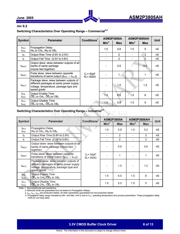
Guaranteed low skew < 500pS (max.)
Very low duty cycle distortion < 1.0nS (max)
Very low CMOS power levels
TTL compatible inputs and outputs
Inputs can be driven from 3.3V or 5V components
Two independent output banks with 3-state control
1:5 fanout per bank
"Heartbeat" monitor output
V
CC
= 3.3V 鹵 0.3V
Available in SSOP, SOIC and QSOP Packages
ASM2P3805AH
Functional Description
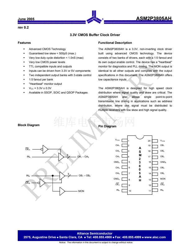
The ASM2P3805AH is a 3.3V, non-inverting clock driver
built using advanced CMOS technology. The device
consists of two banks of drivers, each with a 1:5 fanout and
its own output enable control. The device has a "heartbeat"
monitor for diagnostics and PLL driving. The MON output is
identical to all other outputs and complies with the output
specifications in this document. The ASM2P3805AH offers
low capacitance inputs.
The ASM2P3805AH is designed for high speed clock
distribution where signal quality and skew are critical. The
ASM2P3805AH
also
allows
single
point-to-point
transmission line driving in applications such as address
distribution, where one signal must be distributed to
multiple receivers with low skew and high signal quality.
Block Diagram
Pin Diagram
V
CCA
OA
1
1
2
3
4
5
6
7
8
9
10
20
V
CCB
OB
1
OB
2
OB
3
GND
B
OB
4
OB
5
MON
OE
B
IN
B
OE
A
IN
A
5
OA
1
鈥?OA
5
OA
2
OA
3
GND
A
OA
4
IN
B
OE
B
5
OB
1
鈥?OB
5
OA
5
GND
Q
OE
A
A
S
M
2
3
8
0
5
A
H
19
18
17
16
15
14
13
12
11
MON
IN
A
Alliance Semiconductor
2575, Augustine Drive
鈥?/div>
Santa Clara, CA
鈥?/div>
Tel: 408.855.4900
鈥?/div>
Fax: 408.855.4999
鈥?/div>
www.alsc.com
Notice: The information in this document is subject to change without notice.


 1
1
 2
2
 3
3
 4
4
 5
5
 6
6
 7
7
 8
8
 9
9
 10
10
 11
11
 12
12
 13
13
