Suggested PCB Land Pattern Designs for
Leaded and Leadless Packages and Detailed
Surface Mount Guidelines for Leadless Packages
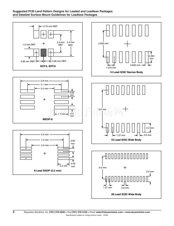
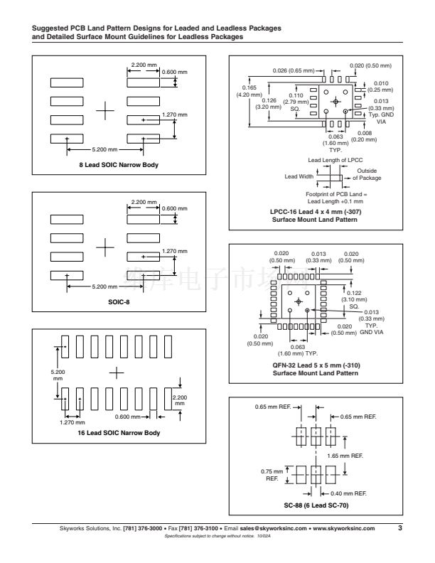
Below are sample printed circuit board land pattern
dimensions. These are based on the IPC (Institute for
Interconnecting and Packaging Electronic Circuits) surface
mount design and land pattern standard: IPC-SM-782.
These drawings are for reference only. It is recommended
that you consult with the company doing the component
mounting and soldering to the printed circuit board. These
companies have more information on options (various
possible dimensions) of actual land patterns.
375
碌m
0.051 (1.30 mm)
0.026
(0.65 mm)
0.087
(2.20 mm)
0.055
(1.40 mm)
0.020 (0.50 mm)
SC-70
600
碌m
0.075
(1.90 mm)
0.037
(0.95 mm)
250
碌m
Chip Scale
0.087
(2.20 mm)
0.055
(1.40 mm)
0.014
(0.35 mm) NOM.
0.039
(1.00 mm)
0.014 (0.35 mm) NOM.
SOT-23 3 Lead
0.053
(1.35 mm) NOM.
SC-79
0.075 (1.90 mm)
0.095 (2.40 mm)
0.030
(0.80 mm)
0.087
(2.20 mm)
0.067
(1.70 mm)
0.031 (0.80 mm)
0.057 (1.44 mm)
0.035
(0.90 mm)
0.039 (1.00 mm) MIN.
0.039
0.047 (1.20 mm) MAX. (1.00 mm)
SOD-323
SOT-143
Skyworks Solutions, Inc.
[781] 376-3000
鈥?/div>
Fax
[781] 376-3100
鈥?/div>
Email
sales@skyworksinc.com
鈥?/div>
www.skyworksinc.com
Specifications subject to change without notice. 10/02A
1


 1
1
 2
2
 3
3
 4
4
 5
5
