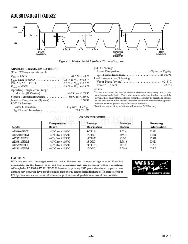
a
+2.5 V to +5.5 V, 120 A, 2-Wire Interface,
Voltage Output 8-/10-/12-Bit DACs
AD5301/AD5311/AD5321*
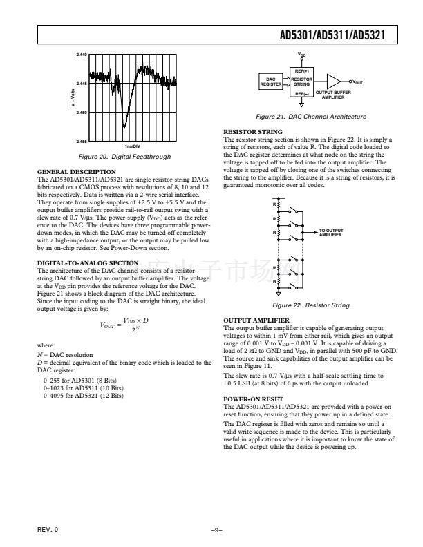
GENERAL DESCRIPTION
FEATURES
AD5301: Buffered Voltage Output 8-Bit DAC
AD5311: Buffered Voltage Output 10-Bit DAC
AD5321: Buffered Voltage Output 12-Bit DAC
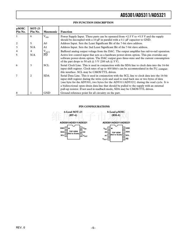
6-Lead SOT-23 and 8-Lead SOIC Packages
Micropower Operation: 120 A @ 3 V
2-Wire (I
2
C
廬
Compatible) Serial Interface
Data Readback Capability
+2.5 V to +5.5 V Power Supply
Guaranteed Monotonic By Design Over All Codes
Power-Down to 50 nA @ 3 V
Reference Derived from Power Supply
Power-On-Reset to Zero Volts
On-Chip Rail-to-Rail Output Buffer Amplifier
Three Power-Down Functions
APPLICATIONS
Portable Battery Powered Instruments
Digital Gain and Offset Adjustment
Programmable Voltage and Current Sources
Programmable Attenuators
The AD5301/AD5311/AD5321 are single 8-, 10- and 12-bit
buffered voltage-output DACs that operate from a single +2.5 V
to +5.5 V supply consuming 120
碌A(chǔ)
at 3 V. The on-chip output
amplifier allows rail-to-rail output swing with a slew rate of
0.7 V/碌s. It uses a 2-wire (I
2
C compatible) serial interface that
operates at clock rates up to 400 kHz. Multiple devices can
share the same bus.
The reference for the DAC is derived from the power supply
inputs and thus gives the widest dynamic output range. These
parts incorporate a power-on-reset circuit, which ensures that
the DAC output powers-up to zero volts and remains there until
a valid write takes place. The parts contain a power-down feature
which reduces the current consumption of the device to 50 nA
at 3 V and provides software-selectable output loads while in
power-down mode.
The low power consumption in normal operation make these
DACs ideally suited to portable battery-operated equipment.
The power consumption is 0.75 mW at 5 V, 0.36 mW at 3 V
reducing to 1
碌W
in all power-down modes.
FUNCTIONAL BLOCK DIAGRAM
V
DD
AD5301/AD5311/AD5321
REF
SCL
SDA
A0
A1*
POWER-DOWN
LOGIC
RESISTOR
NETWORK
INTERFACE
LOGIC
DAC
REGISTER
8-/10-/12-BIT
DAC
BUFFER
V
OUT
POWER-ON
RESET
GND
*AVAILABLE ON 8-LEAD VERSION ONLY
PD*
I
2
C is a registered trademark of Philips Corporation.
*Protected by U.S. Patent No. 5684481, other patent pending.
REV. 0
Information furnished by Analog Devices is believed to be accurate and
reliable. However, no responsibility is assumed by Analog Devices for its
use, nor for any infringements of patents or other rights of third parties
which may result from its use. No license is granted by implication or
otherwise under any patent or patent rights of Analog Devices.
One Technology Way, P.O. Box 9106, Norwood, MA 02062-9106, U.S.A.
Tel: 781/329-4700
World Wide Web Site: http://www.analog.com
Fax: 781/326-8703
漏 Analog Devices, Inc., 1999


 1
1
 2
2
 3
3
 4
4
 5
5
 6
6
 7
7
 8
8
 9
9
 10
10
 11
11
 12
12
 13
13
 14
14
 15
15
