SN74LVC161284
19 BIT BUS INTERFACE
SCAS583J 鈭?NOVEMBER 1996 鈭?REVISED FEBRUARY 2005
D
1.4-k鈩?Pullup Resistors Integrated on All
D
D
D
D
Open-Drain Outputs Eliminate the Need for
Discrete Resistors
ESD Protection Exceeds 2000 V Per
MIL-STD-883, Method 3015; Exceeds 200 V
Using Machine Model (C = 200 pF, R = 0)
Designed for the IEEE Std 1284-I (Level 1
Type) and IEEE Std 1284-II (Level 2 Type)
Electrical Specifications
Flow-Through Architecture Optimizes PCB
Layout
Package Options Include Plastic 300-mil
Shrink Small-Outline (DL) and Thin-Shrink
Small-Outline (DGG) Packages
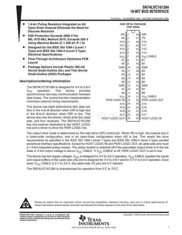
DGG OR DL PACKAGE
(TOP VIEW)
description/ordering information
The SN74LVC161284 is designed for 3-V to 3.6-V
V
CC
operation.
This
device
provides
asynchronous two-way communication between
data buses. The control-function implementation
minimizes external timing requirements.
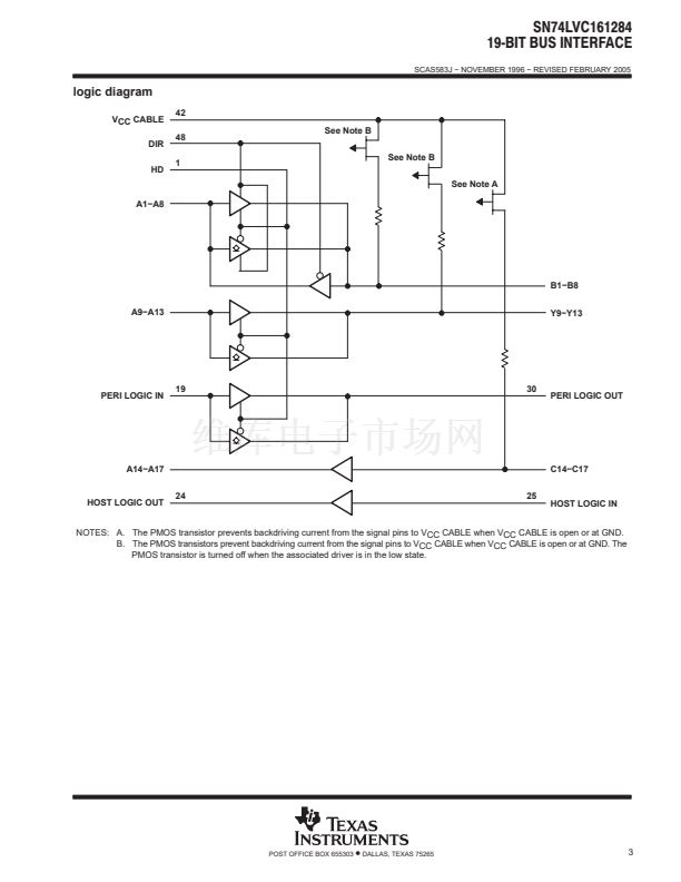
This device has eight bidirectional bits; data can
flow in the A-to-B direction when DIR is high and
in the B-to-A direction when DIR is low. This
device also has five drivers, which drive the cable
side, and four receivers. The SN74LVC161284
has one receiver dedicated to the HOST LOGIC
line and a driver to drive the PERI LOGIC line.
HD
A9
A10
A11
A12
A13
V
CC
A1
A2
GND
A3
A4
A5
A6
GND
A7
A8
V
CC
PERI LOGIC IN
A14
A15
A16
A17
HOST LOGIC OUT
1
2
3
4
5
6
7
8
9
10
11
12
13
14
15
16
17
18
19
20
21
22
23
24
48
47
46
45
44
43
42
41
40
39
38
37
36
35
34
33
32
31
30
29
28
27
26
25
DIR
Y9
Y10
Y11
Y12
Y13
V
CC
CABLE
B1
B2
GND
B3
B4
B5
B6
GND
B7
B8
V
CC
CABLE
PERI LOGIC OUT
C14
C15
C16
C17
HOST LOGIC IN
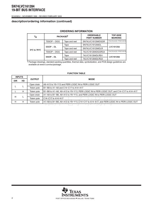
The output drive mode is determined by the high-drive (HD) control pin. When HD is high, the outputs are in
a totem-pole configuration, and in an open-drain configuration when HD is low. This meets the drive
requirements as specified in the IEEE Std 1284-I (level 1 type) and IEEE Std 1284-II (level 2 type) parallel
peripheral-interface specifications. Except for HOST LOGIC IN and PERI LOGIC OUT, all cable-side pins have
a 1.4-k鈩?integrated pullup resistor. The pullup resistor is switched off if the associated output driver is in the low
state or if the output voltage is above V
CC
CABLE. If V
CC
CABLE is off, PERI LOGIC OUT is set to low.
The device has two supply voltages. V
CC
is designed for 3-V to 3.6-V operation. V
CC
CABLE supplies the inputs
and output buffers of the cable side only and is designed for 3-V to 3.6-V and for 4.7-V to 5.5-V operation. Even
when V
CC
CABLE is 3 V to 3.6 V, the cable-side I/O pins are 5-V tolerant.
The SN74LVC161284 is characterized for operation from 0擄C to 70擄C.
Please be aware that an important notice concerning availability, standard warranty, and use in critical applications of
Texas Instruments semiconductor products and disclaimers thereto appears at the end of this data sheet.
PRODUCTION DATA information is current as of publication date.
Products conform to specifications per the terms of Texas Instruments
standard warranty. Production processing does not necessarily include
testing of all parameters.
Copyright
錚?/div>
2005 Texas Instruments Incorporated
POST OFFICE BOX 655303
鈥?/div>
DALLAS, TEXAS 75265
1


 1
1
 2
2
 3
3
 4
4
 5
5
 6
6
 7
7
 8
8
 9
9
 10
10
 11
11
 12
12
