鈥?/div>
Military and Space
High Reliability Systems
Voltage Level Shifting
Isolated Receiver Inputs
Communication Systems
DESCRIPTION
Radiation tests performed on the 66099 optocoupler have shown that the electrical performance of the device after irradiation
is an order of magnitude better than the 4N49 optocouplers. The 66191 has the same components and layout in a 6 pin,
hermetically sealed leadless chip carrier package. Figures 1 and 2 from the 66099 data sheet illustrate the radiation
performance of the device
ABSOLUTE MAXIMUM RATINGS (t
a
= 25擄C unless otherwise noted)
Storage Temperature..........................................................................................................................................-55擄C to +150擄C
Operating Free-Air Temperature Range.............................................................................................................-55擄C to +100擄C
Lead Solder Temperature (10 seconds max)......................................................................................................................240擄C
Input to output Isolation Voltage.........(see Note 1)...........................................................................................................+1kVdc
*
Input Diode
Peak Forward Input Current................................................................. .............................................................................. 50mA
Reverse Input Voltage...............................................................................................................................................................7V
Input Power Dissipation.......................(see Note 2)............................................................................................................80mW
*Output
Photodetector
Continuous Collector Current................... ...........................................................................................................................50mA
Collector-Emitter Voltage........................................................................................................................................................ 40V
Emitter-Collector Voltage.......................................................................................................................................................... 5V
Collector-Base Voltage............................................................................................................................................................40V
Power Dissipation...............................(see Note 3)...........................................................................................................300mW
Notes:
1. Measured with input diode leads shorted together and output leads shorted together
2. Derate linearly 0.80mW/擄C above 25擄C.
3. Derate linearly 3.0mW/擄C above 25擄C.
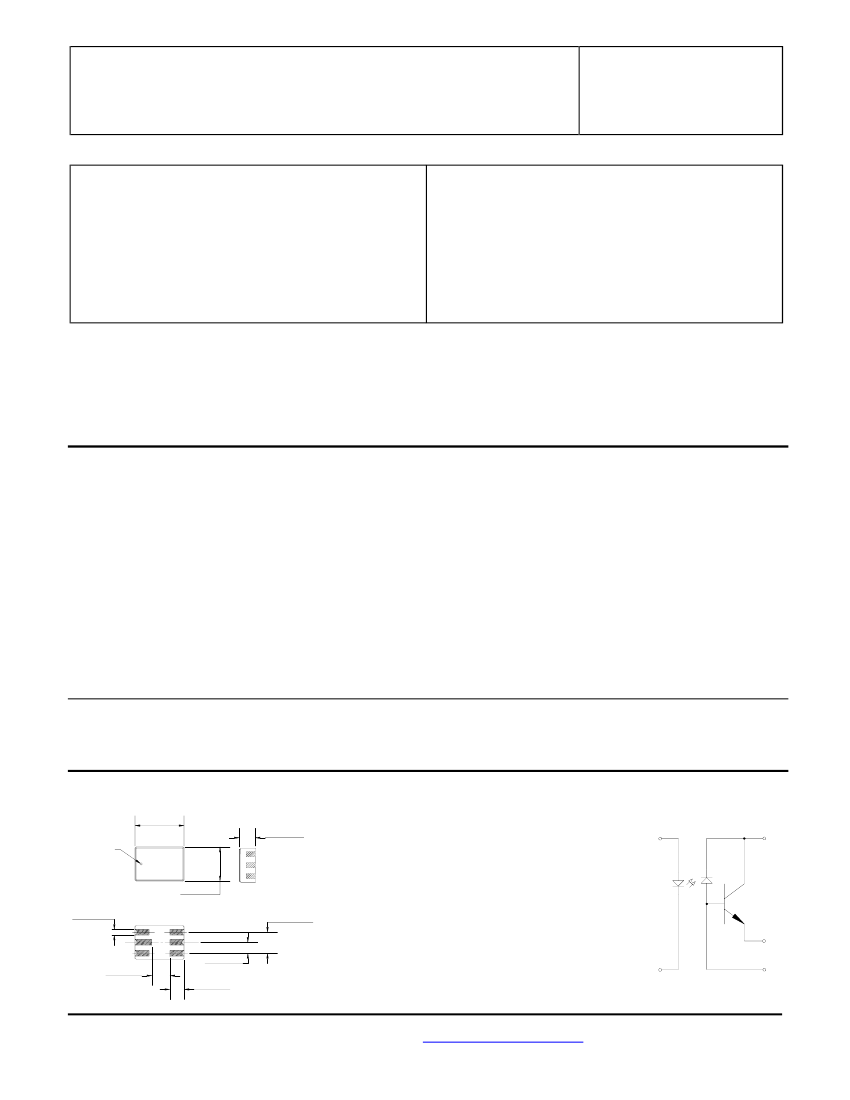
Package Dimensions
0.253 [6.42]
0.237 [6.01]
PIN 1
IDENTIFIER
Schematic Diagram
0.087 [2.22]
0.071 [1.81]
1
C
3
0.178 [4.52]
0.162 [4.11]
0.036 [0.91]
0.020 [0.51]
0.113 [2.87]
0.097 [2.46]
2
1
6
3
4
5
0.055 [1.40]
0.045 [1.14]
0.078 [1.99]
0.062 [1.58]
E
6
B
5
4
0.098 [2.49]
0.082 [2.08]
MICROPAC INDUSTRIES, INC. OPTOELECTRONIC PRODUCTS DIVISION
鈥?/div>
725 E. Walnut St., Garland, TX 75040
鈥?/div>
(972) 272-3571
鈥?/div>
Fax (972) 487-6918
www.micropac.com
E-MAIL:
optosales@micropac.com
5 - 40


 1
1
 2
2
