鈥?/div>
Eliminate ground loops
Level shifting
Line receiver
Switching power supplies
Motor control
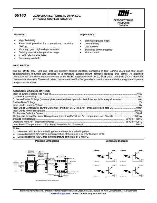
DESCRIPTION
The Mii
66143
-002, -003 and -004 are optically coupled isolators, consisting of four GaAlAs LEDs and four silicon
phototransistors mounted and coupled in a miniature surface mount hermetic leadless chip carrier. All electrical
characteristics of each channel are identical to the JEDEC registered 4N47 (-002), 4N48 (-003) and 4N49 (-004). Each unit
contains four channels. These solid state couplers are ideal for designs where board space and device weight are important
design considerations.
ABSOLUTE MAXIMUM RATINGS
Input-to-output Voltage (see Note 1).....................................................................................................................................+1kV
Collector-Base Voltage ...........................................................................................................................................................45V
Collector-Emitter Voltage (Value applies to emitter-base open-circuited & the input-diode equal to zero) ..........................40V
Emitter-Base Voltage ................................................................................................................................................................7V
Input Diode Reverse Voltage ...................................................................................................................................................3V
Input Diode Continuous Forward Current at (or below) 65擄C Free-Air Temperature (see note 2).....................................40mA
Input Diode Power Dissipation........................................................................................................................................... 60mW
Continuous Collector Current...............................................................................................................................................50mA
Continuous Transistor Power Dissipation at (or below) 25擄C Free-Air Temperature (see Note 3)................................ 300mW
Storage Temperature ........................................................................................................................................ -65擄C to +150擄C
Operating Free-Air Temperature Range............................................................................................................ -55擄C to +125擄C
Lead Solder Temperature (1/16鈥?(1.6mm) from case for 10 seconds)...............................................................................240擄C
Notes:
1. Measured with Inputs shorted together and outputs shorted together.
2. Derate linearly to 125擄C free-air temperature at the rate of 0.67 mA/擄C above 65擄C.
3. Derate linearly to 125擄C free-air temperature at the rate of 3 mW/擄C.
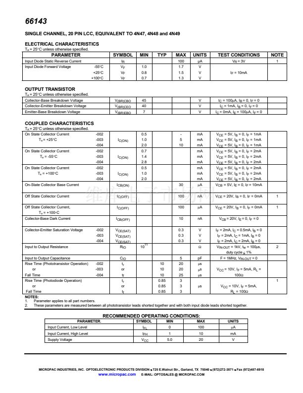
Package Dimensions
Schematic Diagram
0.350 [8.89]
+0.010 [0.25]
-.005[0.13] SQ.
0.200 [5.08]SQ.
0.240 [6.10]SQ.
A 8
.003
0.066 [1.68]
.002
0.025 [0.64]
0.020 [0.51]
.020 X 45擄
.002
0.025 鹵.003
0.200 [5.08]
TYP
0.053 [1.34]
11 C
A 3
6 C
K 7
A 13
0.314 [7.98]
鹵.004 [0.10]
SQ.
0.250 [6.35]
鹵.006 [0.15]
SQ.
10 E
9 B
16 C
K 2
A 17
5 E
4
B
1 C
Mii 66171
XXXXX
NO. 1 LEAD
0.075 [1.91]
NO. 1 LEAD
.040 X 45 擄 (3 PL)
R0.008 [R0.20]TYP
0.075 [1.91]
REF
0.050 [1.27]
TYP
K 12
15 E
14
B
K 18
20 E
19
B
ALL DIMENSIONS ARE IN INCHES [MILLIMETERS]
MICROPAC INDUSTRIES, INC. OPTOELECTRONIC PRODUCTS DIVISION
鈥?/div>
725 E.Walnut Str., Garland, TX 75040
鈥?/div>
(972)272-3571
鈥?/div>
Fax (972)487-6918
www.micropac.com
E-MAIL: OPTOSALES @ MICROPAC.COM


 1
1
 2
2
