54FCT377 Octal D-Type Flip-Flop with Clock Enable
October 1999
54FCT377
Octal D-Type Flip-Flop with Clock Enable
General Description
The 鈥橣CT377 has eight edge-triggered, D-type flip-flops with
individual D inputs and Q outputs. The common buffered
Clock (CP) input loads all flip-flops simultaneously, when the
Clock Enable (CE) is LOW.
The register is fully edge-triggered. The state of each D in-
put, one setup time before the LOW-to-HIGH clock transi-
tion, is transferred to the corresponding flip-flop鈥檚 Q output.
The CE input must be stable only one setup time prior to the
LOW-to-HIGH clock transition for predictable operation.
Features
n
Clock enable for address and data synchronization
applications
n
Eight edge-triggered D flip-flops
n
Buffered common clock
n
See 鈥橣CT273 for master reset version
n
See 鈥橣CT373 for transparent latch version
n
See 鈥橣CT374 for TRI-STATE
廬
version
n
TTL input and output level compatible
n
CMOS power consumption
n
Output sink capability of 32 mA, source capability of
12 mA
n
Standard Microcircuit Drawing (SMD) 5962-8762701
Ordering Code
Military
54FCT377DMQB
54FCT377FMQB
54FCT377LMQB
Package
Number
J20A
W20A
E20A
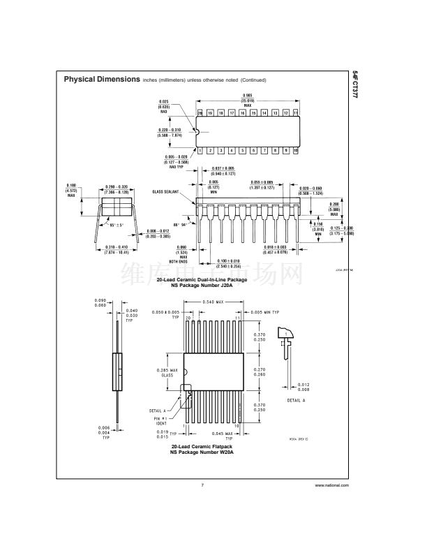
20-Lead Ceramic Dual-In-Line
20-Lead Cerpack
20-Lead Ceramic Leadless Chip Carrier, Type C
Package Description
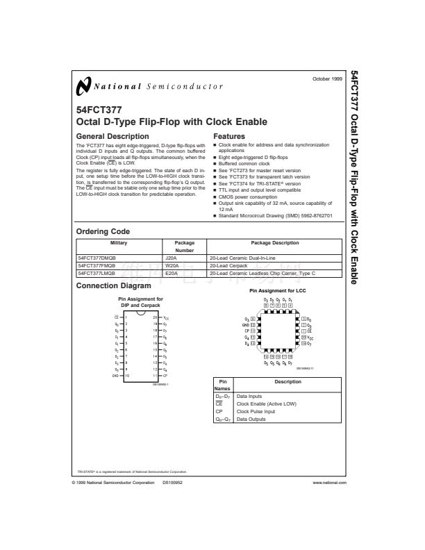
Connection Diagram
Pin Assignment for
DIP and Cerpack
Pin Assignment for LCC
DS100952-11
DS100952-1
Pin
Names
D
0
鈥揇
7
CE
CP
Q
0
鈥換
7
Data Inputs
Description
Clock Enable (Active LOW)
Clock Pulse Input
Data Outputs
TRI-STATE
廬
is a registered trademark of National Semiconductor Corporation.
漏 1999 National Semiconductor Corporation
DS100952
www.national.com


 1
1
 2
2
 3
3
 4
4
 5
5
 6
6
 7
7
 8
8
