HCC/HCF4000B-4001B
HCC/HCF4002B-4025B
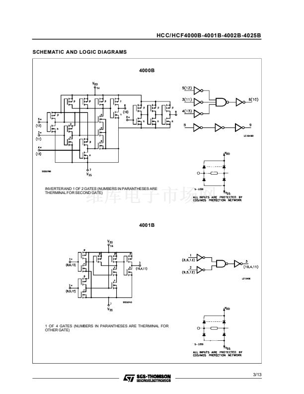
NOR GATE
4000B鈥揇UAL 3 INPUT PLUS INVERTER
4001B鈥換UAD 2 INPUT
4002B-DUAL 4 INPUT
4025B TRIPLE 3 INPUT
micropackage.
The
HCC/HCF4000B, HCC/HCF4001B, HCC/HCF
4002B
and
HCC/HCF4025B
nor gate provide the
system designer with direct implementation of the
nor function and supplement the existing family of
COS/MOS gates. All inputs and outputs are buf-
fered.
.
.
.
.
.
.
.
.
PROPAGATION DELAY TIME = 60 ns (typ.) AT
C
L
= 50 pF, V
DD
= 10 V
BUFFERED INPUTS AND OUTPUTS
STANDARDIZED SYMMETRICAL OUTPUT
CHARACTERISTICS
QUIESCENT CURRENT SPECIFIED TO 20 V
FOR HCC DEVICE
5V, 10V AND 15V PARAMETRIC RATINGS
INPUT CURRENT OF 100nA AT 18V AND 25
o
C
FOR HCC DEVICE
100% TESTED FOR QUIESCENT CURRENT
MEETS ALL REQUIREMENTS OF JEDEC TEN-
TATIVE STANDARD N. 13A, 鈥?STANDARD
SPECIFICATIONS FOR DESCRIPTION OF B
SERIES CMOS DEVICES 鈥?/div>
EY
(Plastic Package)
F
(Ceramic Package)
DESCRIPTION
The
HCC4000B, HCC4001B, HCC4002B
and
HCC4025B
(extended temperature range) and
HCF4000B,
HCF4001B,
HCF4002B
and
HCF4025B
(intermediate temperature range) are
monolithic integrated circuit, available in 14-lead
dual in line plastic or ceramic package and plastic
PIN CONNECTIONS
4000B
4001B
4002B
4025B
M1
(Micro Package)
C1
(Chip Carrier)
ORDER CODES :
HCCXXXXBF
HCFXXXXBM1
HCFXXXXBEY
HCFXXXXBC1
September 1988
1/13


 1
1
 2
2
 3
3
 4
4
 5
5
 6
6
 7
7
 8
8
 9
9
 10
10
 11
11
 12
12
 13
13
