鈥?/div>
Bit rate transparency
High output power
Wide wavelength range
Wide operating case temperature
Built in control electronics with digital interface
Automatic shut-down with enable
Built in input & output signal monitoring
Built in input & output optical isolation
Single 1480 nm pumped
High reliability
Small size
Optical characteristics
Parameter
Wavelength bandwidth
Output power 10 dBm module
Output power 13 dBm module
Output power 16 dBm module
Noise figure
Output power temp. sensitivity
Output power regulation stability
Polarization sensitivity
Input/output return loss
Time response to shut down
Time between SD command and Pout < - 40 dBm
(Case temperature = 0 to + 65 擄C) otherwise specified
Pin > - 6 dBm
Pin > - 6 dBm
Pin > - 6 dBm
1550 nm - 6 dBm input
1550 nm - 6 dBm input (ref. = + 25 擄C)
1550 nm , input from -6 to +4 dBm (ref. = + 25 擄C)
Conditions
Symbol
BW
Pout
Pout
Pout
NF
蠎P/蠎T
蠎P/蠎Pin
蠎P/蠎Pol
R1
SDT
Min
1530
10
13
16
- 0.5
- 0.5
- 0.5
27
Typical
12
15
17
7
Max
1565
14
17
19
10
+ 0.5
+ 0.5
+ 0.5
Unit
nm
dBm
dBm
dBm
dB
dB
dB
dB
dB
mS
40
30
100
Electrical characteristics
Parameter
Positive power supply voltage
Negative power supply voltage
Positive power supply current
Temperature monitoring
Laser drive current monitoring
Alarms Active level
Alarms Non Active level
Shut down (external or automatic)
Typ. value at + 25 擄C
Offset (+ 25 擄C) = 1.2
鹵
0.3 V
Offset = 0 V
Isink < 3 mA for: LIS, LOS1, LOS2 Ibias, TOR
Iscr > - 0.1 mA for: LIS, LOS1, LOS2 Ibias, TOR
Command active
Negative power supply current Max. value at + 65 擄C
Conditions
Symbol
Vcc
Vee
Icc
Iee
Temp
Ipump
Alarm
No alarm
ON
OFF
-6
0.9
0
4.25
3.7
0
Min
4.75
- 5.45
0.45
0.25
-5
1
Typical
Max
5.25
- 4.9
0.9
1
-4
1.1
0.7
5.25
5.25
1.35
Unit
V
V
A
A
擄C/V
A/V
V
V
V
V
For SD and ASD
Command NON Active
(Case temperature = + 25 擄C)
Absolute maximum ratings
Parameter
Symbol
Min
Max
+ 65
+70
+ 350
5
7
0
Unit
擄C
擄C
擄C
N
mm
V
V
Operating temperature
Top
0
Storage temperature
Tstq
-40
Soldering temperature (3s)
Axial pull force on fiber (10s)
F
Fiber bend radius from package
r
40
Positive supply voltage
Vcc
0
Negative supply voltage
Vee
-7
Stresses in excess of the absolute maximum ratings can cause permanent damage to the device.


 1
1
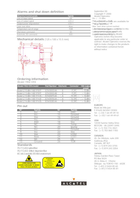 2
2
 3
3
