Transistor
2SD661, 2SD661A
Silicon NPN epitaxial planer type
For low-frequency and low-noise amplification
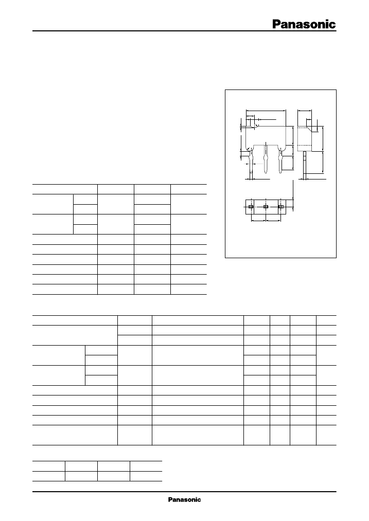
Unit: mm
6.9鹵0.1
1.5
2.5鹵0.1
1.0
1.0
2.4鹵0.2 2.0鹵0.2 3.5鹵0.1
s
q
q
q
Features
Low noise voltage NV.
High foward current transfer ratio h
FE
.
M type package allowing easy automatic and manual insertion as
well as stand-alone fixing to the printed circuit board.
(Ta=25藲C)
Ratings
35
55
35
55
7
200
100
400
150
鈥?5 ~ +150
Unit
1.5 R0.9
R0.9
0.4
1.0鹵0.1
R
0.
0.85
Parameter
Collector to
base voltage
Collector to
2SD661
2SD661A
2SD661
Symbol
V
CBO
V
CEO
V
EBO
I
CP
I
C
P
C
T
j
T
stg
3
2
1
V
2.5
2.5
emitter voltage 2SD661A
Emitter to base voltage
Peak collector current
Collector current
Collector power dissipation
Junction temperature
Storage temperature
V
V
mA
mA
mW
藲C
藲C
1:Base
2:Collector
3:Emitter
EIAJ:SC鈥?1
M Type Mold Package
s
Electrical Characteristics
Parameter
Collector cutoff current
Collector to base
voltage
Collector to emitter
voltage
2SD661
2SD661A
2SD661
2SD661A
(Ta=25藲C)
Symbol
I
CBO
I
CEO
V
CBO
V
CEO
V
EBO
h
FE*
V
CE(sat)
f
T
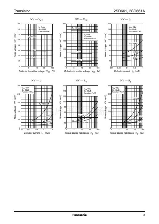
NV
Conditions
V
CB
= 20V, I
E
= 0
V
CE
= 20V, I
B
= 0
I
C
= 10碌A, I
E
= 0
I
C
= 2mA, I
B
= 0
I
E
= 10碌A, I
C
= 0
V
CE
= 10V, I
C
= 2mA
I
C
= 100mA, I
B
= 10mA
V
CB
= 10V, I
E
= 鈥?mA, f = 200MHz
V
CE
= 10V, I
C
= 1mA, G
V
= 80dB
R
g
= 100k鈩? Function = FLAT
200
150
35
55
35
55
7
210
650
1
V
MHz
mV
min
typ
max
0.1
1
Unit
碌A
碌A
V
1.25鹵0.05
s
Absolute Maximum Ratings
0.55鹵0.1
0.45鹵0.05
4.1鹵0.2
4.5鹵0.1
7
V
V
Emitter to base voltage
Forward current transfer ratio
Collector to emitter saturation voltage
Transition frequency
Noise voltage
*
h
FE
Rank classification
R
210 ~ 340
S
290 ~ 460
T
360 ~ 650
h
FE
Rank
1


 1
1
 2
2
 3
3
