Transistor
2SD1996
Silicon NPN epitaxial planer type
For low-voltage output amplification
For muting
For DC-DC converter
0.15
Unit: mm
6.9鹵0.1
0.7
4.0
1.05 2.5鹵0.1
(1.45)
鹵0.05
0.8
s
Features
q
q
q
q
0.65 max.
14.5鹵0.5
0.45
鈥?.05
+0.1
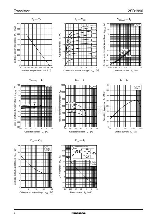
Low collector to emitter saturation voltage V
CE(sat)
.
Low ON resistance R
on
.
High foward current transfer ratio h
FE
.
Allowing supply with the radial taping.
0.45
鈥?.05
2.5鹵0.5
1
2
2.5鹵0.5
3
+0.1
Parameter
Collector to base voltage
Collector to emitter voltage
Emitter to base voltage
Peak collector current
Collector current
Collector power dissipation
Junction temperature
Storage temperature
Symbol
V
CBO
V
CEO
V
EBO
I
CP
I
C
P
C
T
j
T
stg
Ratings
25
20
12
1
0.5
600
150
鈥?5 ~ +150
Unit
V
V
V
A
A
mW
藲C
藲C
0.45
+0.1
鈥?0.05
1.2鹵0.1
0.65
max.
Note: In addition to the
lead type shown in
the upper figure, the
type as shown in
the lower figure is
also available.
1:Emitter
2:Collector
3:Base
MT1 Type Package
2.5鹵0.1
s
Absolute Maximum Ratings
(Ta=25藲C)
0.85
1.0
s
Electrical Characteristics
(Ta=25藲C)
Parameter
Symbol
I
CBO
V
CBO
V
CEO
V
EBO
h
FE1*1
h
FE2
V
CE(sat)
V
BE(sat)
f
T
C
ob
R
on*3
*3
R
on
(HW type)
Conditions
V
CB
= 25V, I
E
= 0
I
C
= 10碌A(chǔ), I
E
= 0
I
C
= 1mA, I
B
= 0
I
E
= 10碌A(chǔ), I
C
= 0
V
CE
= 2V, I
C
= 0.5A
*2
V
CE
= 2V, I
C
= 1A
*2
I
C
= 0.5A, I
B
= 20mA
I
C
= 0.5A, I
B
= 50mA
V
CB
= 10V, I
E
= 鈥?0mA, f = 200MHz
V
CB
= 10V, I
E
= 0, f= 1MHz
min
typ
max
100
Collector cutoff current
Collector to base voltage
Collector to emitter voltage
Emitter to base voltage
Forward current transfer ratio
Collector to emitter saturation voltage
Base to emitter saturation voltage
Transition frequency
Collector output capacitance
ON resistanse
3.5鹵0.1
0.8
Unit
nA
V
V
V
25
20
12
200
60
0.13
0.4
1.2
200
10
1.0
*2
800
V
V
MHz
pF
鈩?/div>
Measurement circuit
1k鈩?/div>
Pulse measurement
*1
h
FE1
Rank classification
I
B
=1mA
Rank
h
FE1
R
200 ~ 350
S
300 ~ 500
T
400 ~ 800
R
on
=
V
B
V
V
V
A
f=1kHz
V=0.3V
V
B
!1000(鈩?
V
A
鈥揤
B
1


 1
1
 2
2
 3
3
