'$7$ 6+((7
SILICON POWER TRANSISTOR
2SD1588
NPN SILICON EPITAXIAL TRANSISTOR
FOR LOW-FREQUENCY POWER AMPLIFIERS AND LOW-SPEED SWITCHING
FEATURES
鈥?Mold package that does not require an insulating board or
insulation bushing
鈥?Large current capacity in small dimension: I
C(DC)
= 7 A
鈥?Low collector saturation voltage: V
CE(sat)
= 0.5 V MAX. (@5 A)
鈥?Ideal for use in ramp drivers or inductance drivers
鈥?Complementary transistor: 2SB1097
PACKAGE DRAWING (UNIT: mm)
ABSOLUTE MAXIMUM RATINGS (T
A
= 25擄C)
擄
Parameter
Collector to base voltage
Collector to emitter voltage
Emitter to base voltage
Collector current (DC)
Collector current (Pulse)
Base current (DC)
Total power dissipation
Total power dissipation
Junction temperature
Storage temperature
Symbol
V
CBO
V
CEO
V
EBO
I
C(DC)
I
C(pulse)
*
I
B(DC)
P
T
(T
C
= 25擄C)
P
T
(T
A
= 25擄C)
T
j
T
stg
Ratings
100
60
7.0
7.0
15
3.5
30
2.0
150
鈭?5
to +150
Unit
V
V
V
A
A
A
W
W
擄C
擄C
(OHFWURGH &RQQHFWLRQ
��! %DVH
��! &ROOHFWRU
��! (PLWWHU
* PW
鈮?/div>
300
碌
s, duty cycle
鈮?/div>
10%
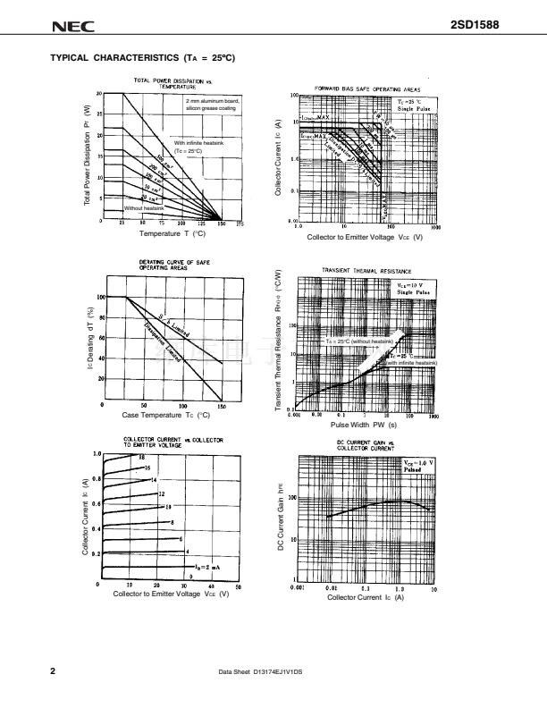
ELECTRICAL CHARACTERISTICS (T
A
= 25擄C)
擄
Parameter
Collector cutoff current
Emitter cutoff current
DC current gain
DC current gain
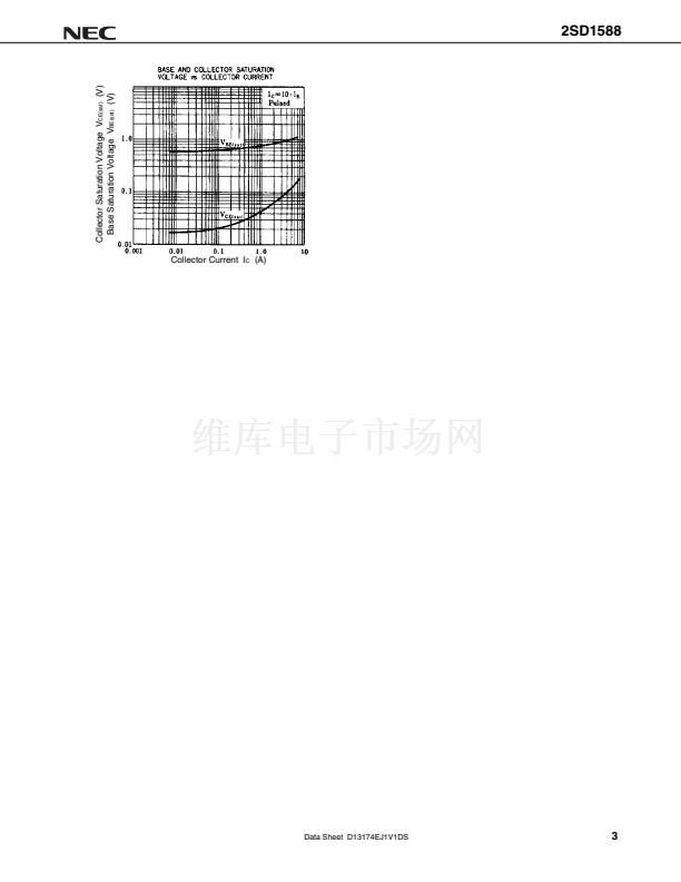
Collector saturation voltage
Base saturation voltage
Symbol
I
CBO
I
EBO
h
FE1
**
h
FE2
**
V
CE(sat)
**
V
BE(sat)
**
Conditions
V
CB
= 80 V, I
E
= 0
V
EB
= 5.0 V, I
C
= 0
V
CE
= 1.0 V, I
C
= 3 A
V
CE
= 1.0 V, I
C
= 5 A
I
C
= 5 A, I
B
= 0.5 A
I
C
= 5 A, I
B
= 0.5 A
40
20
0.5
1.5
V
V
MIN.
TYP.
MAX.
10
10
200
Unit
碌
A
碌
A
** Pulse test PW
鈮?/div>
350
碌
s, duty cycle
鈮?/div>
2%/per pulsed
h
FE
CLASSIFICATION
Marking
h
FE1
M
40 to 80
L
60 to 120
K
100 to 200
The information in this document is subject to change without notice. Before using this document, please
confirm that this is the latest version.
Not all devices/types available in every country. Please check with local NEC representative for
availability and additional information.
Document No. D13174EJ1V1DS00 (1st edition)
Date Published April 2002 N CP(K)
Printed in Japan
漏
2002
1998


 1
1
 2
2
 3
3
 4
4
