Transistor
2SB0767
(2SB767)
Silicon PNP epitaxial planer type
For low-frequency output amplification
Complementary to 2SD0875 (2SD875)
Unit: mm
I
Features
G
G
G
4.5鹵0.1
1.6鹵0.2
1.5鹵0.1
Large collector power dissipation P
C
.
High collector to emitter voltage V
CEO
.
Mini type package, allowing downsizing of the equipment and
automatic insertion through the tape packing and the magazine
packing.
(Ta=25藲C)
Ratings
鈥?0
鈥?0
鈥?
鈥?
鈥?0.5
1
150
鈥?5 ~ +150
Unit
V
V
V
A
A
W
藲C
藲C
2.6鹵0.1
0.4max.
45擄
1.0
鈥?.2
+0.1
0.4鹵0.08
0.5鹵0.08
1.5鹵0.1
3.0鹵0.15
3
2
1
4.0
鈥?.20
0.4鹵0.04
I
Absolute Maximum Ratings
Parameter
Collector to base voltage
Collector to emitter voltage
Emitter to base voltage
Peak collector current
Collector current
Collector power dissipation
Junction temperature
Storage temperature
*
Symbol
V
CBO
V
CEO
V
EBO
I
CP
I
C
P
C*
T
j
T
stg
marking
1:Base
2:Collector
3:Emitter
EIAJ:SC鈥?2
Mini Power Type Package
Marking symbol
: C
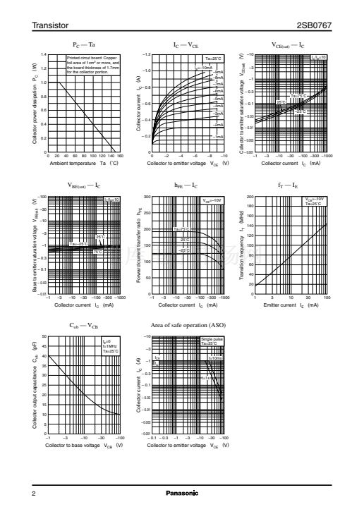
Printed circuit board: Copper foil area of 1cm
2
or more, and the board
thickness of 1.7mm for the collector portion
I
Electrical Characteristics
Parameter
Collector cutoff current
Collector to base voltage
Collector to emitter voltage
Emitter to base voltage
Forward current transfer ratio
Collector to emitter saturation voltage
Base to emitter saturation voltage
Transition frequency
Collector output capacitance
(Ta=25藲C)
Symbol
I
CBO
V
CBO
V
CEO
V
EBO
h
FE1*1
h
FE2
V
CE(sat)
V
BE(sat)
f
T
C
ob
Conditions
V
CB
= 鈥?0V, I
E
= 0
I
C
= 鈥?0碌A(chǔ), I
E
= 0
I
C
= 鈥?00碌A(chǔ), I
B
= 0
I
E
= 鈥?0碌A(chǔ), I
C
= 0
V
CE
= 鈥?0V, I
C
= 鈥?50mA
*2
V
CE
= 鈥?V, I
C
= 鈥?00mA
*2
I
C
= 鈥?00mA, I
B
= 鈥?0mA
*2
I
C
= 鈥?00mA, I
B
= 鈥?0mA
*2
V
CB
= 鈥?0V, I
E
= 50mA, f = 200MHz
V
CB
= 鈥?0V, I
E
= 0, f = 1MHz
鈥?0
鈥?0
鈥?
90
50
100
鈥?0.2
鈥?0.85
120
20
*2
min
typ
max
鈥?0.1
2.5鹵0.1
+0.25
Unit
碌A(chǔ)
V
V
V
330
鈥?.4
鈥?.2
V
V
MHz
30
pF
Pulse measurement
*1
h
FE1
Rank classification
Rank
h
FE1
Q
90 ~ 155
CQ
R
130 ~ 220
CR
S
185 ~ 330
CS
Note.) The Part number in the Parenthesis shows
conventional part number.
Marking Symbol
1


 1
1
 2
2
 3
3
