Transistor
2SB1463
Silicon PNP epitaxial planer type
For high breakdown voltage low-noise amplification
Complementary to 2SD2240
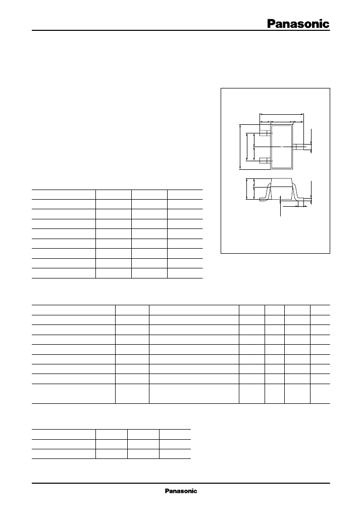
1.6鹵0.15
Unit: mm
s
Features
q
q
q
0.4
0.8鹵0.1
0.4
High collector to emitter voltage V
CEO
.
Low noise voltage NV.
SS-Mini type package, allowing downsizing of the equipment
and automatic insertion through the tape packing and the maga-
zine packing.
(Ta=25藲C)
Ratings
鈥?50
鈥?50
鈥?
鈥?00
鈥?0
125
125
鈥?5 ~ +125
Unit
V
V
V
mA
mA
mW
藲C
藲C
1.6鹵0.1
1.0鹵0.1
0.5
1
0.5
3
2
0.45鹵0.1 0.3
0.75鹵0.15
Parameter
Collector to base voltage
Collector to emitter voltage
Emitter to base voltage
Peak collector current
Collector current
Collector power dissipation
Junction temperature
Storage temperature
Symbol
V
CBO
V
CEO
V
EBO
I
CP
I
C
P
C
T
j
T
stg
1:Base
2:Emitter
3:Collector
EIAJ:SC鈥?5
SS鈥揗ini Type Package
Marking symbol :
I
s
Electrical Characteristics
Parameter
Collector cutoff current
Collector to emitter voltage
Emitter to base voltage
Forward current transfer ratio
Collector to emitter saturation voltage
Transition frequency
Collector output capacitance
Noise voltage
(Ta=25藲C)
Symbol
I
CBO
V
CEO
V
EBO
h
FE
f
T
C
ob
NV
*
Conditions
V
CB
= 鈥?00V, I
E
= 0
I
C
= 鈥?00碌A(chǔ), I
B
= 0
I
E
= 鈥?0碌A(chǔ), I
C
= 0
V
CE
= 鈥?V, I
C
= 鈥?0mA
I
C
= 鈥?0mA, I
B
= 鈥?mA
V
CB
= 鈥?0V, I
E
= 10mA, f = 200MHz
V
CB
= 鈥?0V, I
E
= 0, f = 1MHz
V
CE
= 鈥?0V, I
C
= 鈥?mA, G
V
= 80dB,
R
g
= 100k鈩? Function = FLAT
min
typ
0 to 0.1
0.2鹵0.1
max
鈥?
0.15
鈥?.05
+0.1
s
Absolute Maximum Ratings
0.2
鈥?.05
+0.1
Unit
碌A(chǔ)
V
V
鈥?50
鈥?
130
450
鈥?
200
4
150
V
CE(sat)
V
MHz
pF
mV
*
h
FE
Rank classification
Rank
h
FE
Marking Symbol
R
130 ~ 220
IR
S
185 ~ 330
IS
T
260 ~ 450
IT
1


 1
1
 2
2
 3
3
