鈥?/div>
Device Marking: Logo, Device Type, e.g., 2N6027, Date Code
MAXIMUM RATINGS
(TJ = 25擄C unless otherwise noted)
Rating
*Power Dissipation
Derate Above 25擄C
*DC Forward Anode Current
Derate Above 25擄C
*DC Gate Current
Repetitive Peak Forward Current
100
碌
s Pulse Width, 1% Duty Cycle
*20
碌
s Pulse Width, 1% Duty Cycle
Non鈥揜epetitive Peak Forward Current
10
碌
s Pulse Width
*Gate to Cathode Forward Voltage
*Gate to Cathode Reverse Voltage
*Gate to Anode Reverse Voltage
*Anode to Cathode Voltage(1)
Operating Junction Temperature Range
*Storage Temperature Range
*Indicates JEDEC Registered Data
(1) Anode positive, RGA = 1000 ohms
Anode negative, RGA = open
Symbol
PF
1/胃JA
IT
IG
ITRM
1.0
2.0
ITSM
VGKF
VGKR
VGAR
VAK
TJ
Tstg
5.0
40
Amps
Volts
Volts
Volts
Volts
擄C
擄C
Value
300
4.0
150
2.67
Unit
mW
mW/擄C
mA
mA/擄C
mA
Amps
1
2
3
1
2
http://onsemi.com
PUTs
40 VOLTS
300 mW
G
A
K
3
"
50
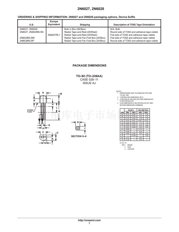
TO鈥?2 (TO鈥?26AA)
CASE 029
STYLE 16
PIN ASSIGNMENT
Anode
Gate
Cathode
*
5.0
"
40
鈥?0 to
+100
鈥?5 to
+150
40
ORDERING INFORMATION
See detailed ordering and shipping information in the package
dimensions section on page 7 of this data sheet.
Preferred
devices are recommended choices for future use
and best overall value.
漏
Semiconductor Components Industries, LLC, 2000
1
May, 2000 鈥?Rev. 2
Publication Order Number:
2N6027/D


 1
1
 2
2
 3
3
 4
4
 5
5
 6
6
 7
7
 8
8
