28LV64A
64K (8K x 8) Low Voltage CMOS EEPROM
FEATURES
鈥?2.7V to 3.6V Supply
鈥?Read Access Time鈥?00 ns
鈥?CMOS Technology for Low Power Dissipation
- 8 mA Active
- 50
碌
A CMOS Standby Current
鈥?Byte Write Time鈥? ms
鈥?Data Retention >200 years
鈥?High Endurance - Minimum 100,000 Erase/Write
Cycles
鈥?Automatic Write Operation
- Internal Control Timer
- Auto-Clear Before Write Operation
- On-Chip Address and Data Latches
鈥?Data Polling
鈥?Ready/Busy
鈥?Chip Clear Operation
鈥?Enhanced Data Protection
- V
CC
Detector
- Pulse Filter
- Write Inhibit
鈥?Electronic Signature for Device Identi鏗乧ation
鈥?Organized 8Kx8 JEDEC Standard Pinout
- 28-pin Dual-In-Line Package
- 32-pin Chip Carrier (Leadless or Plastic)
鈥?Available for Extended Temperature Ranges:
- Commercial: 0藲C to +70藲C
- Industrial: -40藲C to +85藲C
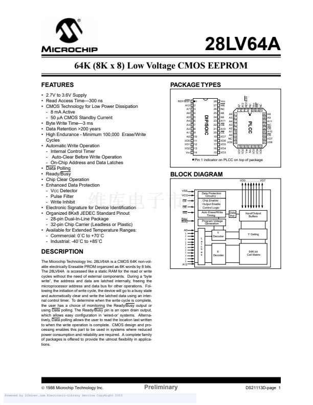
PACKAGE TYPES
RDY/BSY
A12
A7
A6
A5
A4
A3
A2
A1
A0
I/O0
I/O1
I/O2
V
SS
鈥?
2
3
4
5
6
7
8
9
10
11
12
13
14
28
27
26
25
24
23
22
21
20
19
18
17
16
15
Vcc
WE
NC
A8
A6
5
A9
A5
6
A11
A4
7
A3
8
OE
A10
A2
9
A1
10
CE
A0
11
I/O7
NC
12
I/O6
I/O0
13
I/O5
I/O4
I/O3
2
RDY/BSY
1
NU
4
A7
3
A12
32
Vcc
31
WE
18
19
30
NC
29
A8
28
A9
27
A11
26
NC
25
OE
24
A10
23
CE
22
I/O7
21
I/O6
14
15
16
17
鈥?Pin 1 indicator on PLCC on top of package
BLOCK DIAGRAM
I/O0...................I/O7
VSS
VCC
CE
OE
WE
Rdy/
Busy
A0
I
I
I
I
I
I
I
I
I
I
I
A12
Data Protection
Circuitry
Chip Enable/
Output Enable
Control Logic
Auto Erase/Write
Timing
Program Voltage
Generation
Y
Decoder
Data
Poll
Input/Output
Buffers
DESCRIPTION
The Microchip Technology Inc. 28LV64A is a CMOS 64K non-vol-
atile electrically Erasable PROM organized as 8K words by 8 bits.
The 28LV64A is accessed like a static RAM for the read or write
cycles without the need of external components. During a 鈥渂yte
write鈥? the address and data are latched internally, freeing the
microprocessor address and data bus for other operations. Fol-
lowing the initiation of write cycle, the device will go to a busy state
and automatically clear and write the latched data using an inter-
nal control timer. To determine when the write cycle is complete,
the user has a choice of monitoring the Ready/Busy output or
using Data polling. The Ready/Busy pin is an open drain output,
which allows easy con鏗乬uration in 鈥榳ired-or鈥?systems. Alterna-
tively, Data polling allows the user to read the location last written
to when the write operation is complete. CMOS design and pro-
cessing enables this part to be used in systems where reduced
power consumption and reliability are required. A complete family
of packages is offered to provide the utmost 鏗俥xibility in applica-
tions.
L
a
t
c
h
e
s
X
Decoder
漏
1988 Microchip Technology Inc.
Powered by ICminer.com Electronic-Library Service CopyRight 2003
Preliminary
I/O1
I/O2
Vss
NU
I/O3
I/O4
I/O5
Y Gating
64K bit
Cell Matrix
DS21113D-page 1
20
DIP/SOIC
PLCC


 1
1
 2
2
 3
3
 4
4
 5
5
 6
6
 7
7
 8
8
